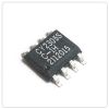
CY23FP12-002

Features: • Pre-programmed Configurations• Fully field-programmable-Input and output dividers-Inverting/noninverting outputs-Phase-locked loop (PLL) or fanout buffer configuration• 10-MHz to 200-MHz operating range• Split 2.5V or 3.3V outputs• Two LVCMOS reference inp...

product image

CY23FP12-002 Picture
SeekIC No. : 004319160 Detail

CY23FP12-002: Features: • Pre-programmed Configurations• Fully field-programmable-Input and output dividers-Inverting/noninverting outputs-Phase-locked loop (PLL) or fanout buffer configuration•...

floor Price/Ceiling Price

Part Number:
CY23FP12-002
Supply Ability:
5000

Price Break

  • Qty
  • 1~5000
  • Unit Price
  • Negotiable
  • Processing time
  • 15 Days
Total Cost: $ 0.00

SeekIC Buyer Protection PLUS - newly updated for 2013!

  • Escrow Protection.
  • Guaranteed refunds.
  • Secure payments.
  • Learn more >>

Month Sales

268 Transactions

Rating

evaluate  (4.8 stars)

Upload time: 2024/11/21

Payment Methods

All payment methods are secure and covered by SeekIC Buyer Protection PLUS.

Notice: When you place an order, your payment is made to SeekIC and not to your seller. SeekIC only pays the seller after confirming you have received your order. We will also never share your payment details with your seller.
Product Details

Description


Features:

• Pre-programmed Configurations
• Fully field-programmable
-Input and output dividers
-Inverting/noninverting outputs
-Phase-locked loop (PLL) or fanout buffer configuration
• 10-MHz to 200-MHz operating range
• Split 2.5V or 3.3V outputs
• Two LVCMOS reference inputs
• Twelve low-skew outputs
-Output-output skew < 200 ps
-Device-device skew < 500 ps
• Input-output skew < 250 ps
• Cycle-cycle jitter < 100 ps (typical)
• Three-stateable outputs
• < 50-A shutdown current
• Spread Aware
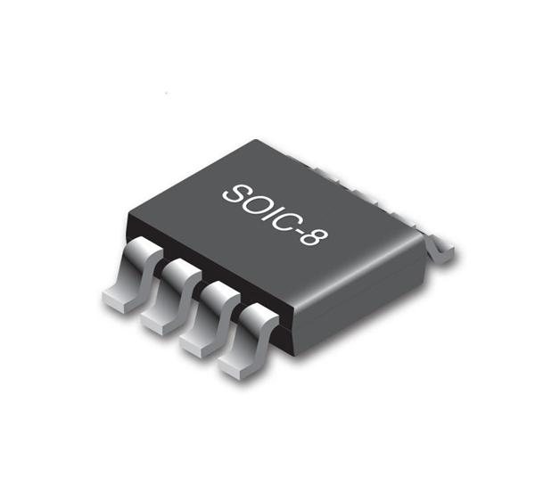
• 28-pin SSOP
• 3.3V operation
• Industrial temperature available


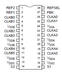
Pinout

  Connection Diagram


Specifications

Parameter Description Condition
Min.
Max.
Unit
VDD Supply Voltage Non-functional
0.5
7
VDC
VIN Input Voltage REF Relative to VCC
0.5
7
VDC
VIN Input Voltage Except REF Relative to VCC
0.5
VDD + 0.5
VDC
LUI Latch-up Immunity Functional
300
mA
TS Temperature, Storage Non-functional
65
+125
°C
TA Temperature, Operating Ambient Commercial Temperature
0
+70
°C
TA Temperature, Operating Ambient Industrial Temperature
40
+85
°C
TJ Junction Temperature Industrial Temperature
125
°C
ØJc Dissipation, Junction to Case Functional
34
°C/W
ØJa Dissipation, Junction to Ambient Functional
86
°C/W
ESDh ESD Protection (Human Body Model)  
2000
V
MSL Moisture Sensitivity Level  
MSL 1
class
GATES Total Functional Gate Count Assembled Die
21375
each
UL94 Flammability Rating @ 1/8 in.
V0
class
FIT Failure in Time Manufacturing test
10
ppm
TPU Power-up time for all VDDs to reach
minimum specified voltage (power
ramps must be monotonic)
 
0.05
500
ms


Description

The CY23FP12-002 is a pre-programmed version of the CY23FP12. It features a high-performance fully field-programmable 200 MHz zero delay buffer designed for high speed clock distribution. The integrated PLL is designed for low jitter and optimized for noise rejection. These parameters are critical for reference clock distribution in systems using highperformance ASICs and microprocessors.

The CY23FP12-002 is fully programmable via volume or prototype programmers enabling the user to define an application- specific Zero Delay Buffer with customized input and output dividers, feedback topology (internal/external), output inversions, and output drive strengths. For additional flexibility, the user can mix and match multiple functions, listed in Table 2, and assign a particular function set to any one of the four possible S1-S2 control bit combinations. This feature allows for the implementation of four distinct personalities, selectable with S1-S2 bits, on a single programmed silicon.

The CY23FP12-002 also features a proprietary auto-powerdown circuit that shuts down the device in case of a REF failure, resulting in less than 50 A of current draw.

The CY23FP12-002 provides twelve outputs grouped in two banks with separate power supply pins which can be connected independently to either a 2.5V or a 3.3V rail. Selectable reference input is a fault tolerance feature which allows for glitch-free switch over to secondary clock source when REFSEL is asserted/de-asserted.


Customers Who Bought This Item Also Bought

Margin,quality,low-cost products with low minimum orders. Secure your online payments with SeekIC Buyer Protection.
View more