Features: • Zero input-output propagation delay, adjustable by capacitive load on FBK input
• Multiple configurations, see "Available CY2308 Configurations" table
• Multiple low-skew outputs
- Output-output skew less than 200 ps
- Device-device skew less than 700 ps
- Two banks of four outputs, three-stateable by two select inputs
• 10-MHz to 133-MHz operating range
• Low jitter, less than 200 ps cycle-cycle (1, 1H, 4, 5H)
• Space-saving 16-pin 150-mil SOIC package or 16-pin TSSOP
• 3.3V operation
• Industrial Temperature availablePinout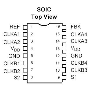 SpecificationsSupply Voltage to Ground Potential ...............0.5V to +7.0V
DC Input Voltage (Except Ref) .............. 0.5V to VDD + 0.5V
DC Input Voltage REF ........................................... 0.5 to 7V
Storage Temperature.................................. 65°C to +150°C
Junction Temperature...................................................150°C
Static Discharge Voltage
(per MIL-STD-883, Method 3015) ............................. >2000VDescriptionThe CY2308 is a 3.3V Zero Delay Buffer designed to distribute high-speed clocks in PC, workstation, datacom, telecom, and other high-performance applications.
The part has an on-chip PLL which locks to an input clock presented on the REF pin. The PLL feedback is required to be driven into the FBK pin, and can be obtained from one of the outputs. The input-to-output skew is guaranteed to be less than 350 ps, and output-to-output skew is guaranteed to be less than 200 ps.
The CY2308 has two banks of four outputs each, which can be controlled by the Select inputs as shown in the table "Select Input Decoding." If all output clocks are not required, Bank B can be three-stated. The select inputs also allow the input clock to be directly applied to the output for chip and system testing purposes.
The CY2308 PLL enters a power-down state when there are no rising edges on the REF input. In this mode, all outputs are three-stated and the PLL is turned off, resulting in less than 50 µA of current draw. The PLL shuts down in two additional cases as shown in the "Select Input Decoding" table.
Multiple CY2308 devices can accept the same input clock and distribute it in a system. In this case, the skew between the outputs of two devices is guaranteed to be less than 700 ps.
The CY2308 is available in five different configurations, as shown in the "Available CY2308 Configurations" table on page 2. The CY23081 is the base part, where the output frequencies equal the reference if there is no counter in the feedback path. The CY23081H is the high-drive version of the 1, and rise and fall times on this device are much faster.
The CY23082 allows the user to obtain 2X and 1X frequencies on each output bank. The exact configuration and output frequencies depends on which output drives the feedback pin. The CY23083 allows the user to obtain 4X and 2X frequencies on the outputs.
The CY23084 enables the user to obtain 2X clocks on all outputs. Thus, the part is extremely versatile, and can be used in a variety of applications.
The CY23085H is a high-drive version with REF/2 on both banks.

 CY2308 Data Sheet