Maximum Input Frequency
:
Minimum Input Frequency
:
Packaging
:
Number of Circuits
: 1
Supply Voltage - Min
: 3 V
Supply Voltage - Max
: 3.6 V
Type
: Zero Delay PLL Clock Buffer
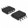
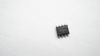
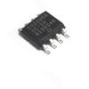
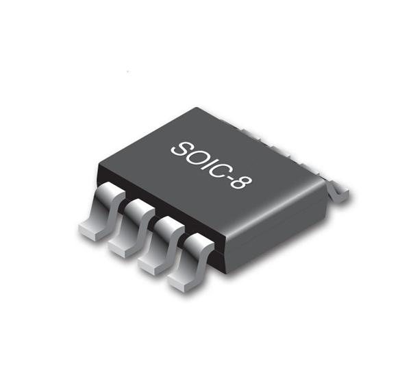
Package / Case
: SOIC-8
Maximum Operating Temperature
: + 70 C
Minimum Operating Temperature
: 0 C
Output Frequency Range
: 10 MHz to 133.33 MHz
Features: • 10-MHz to 100-/133-MHz operating range, compatible
with CPU and PCI bus frequencies
• Zero input-output propagation delay
• Multiple low-skew outputs
-Output-output skew less than 250 ps
-Device-device skew less than 700 ps
-One input drives five outputs (CY2305)
-One input drives nine outputs, grouped as 4 + 4 + 1 (CY2309)
• Less than 200 ps cycle-cycle jitter, compatible with
Pentium-based systems
• Test Mode to bypass phase-locked loop (PLL) (CY2309
only [see "Select Input Decoding" on page 2])
• Available in space-saving 16-pin 150-mil SOIC or
4.4-mm TSSOP packages (CY2309), and 8-pin, 150-mil
SOIC package (CY2305)
• 3.3V operation
• Industrial temperature availablePinout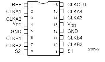 SpecificationsSupply Voltage to Ground Potential ............ 0.5V to +7.0V
DC Input Voltage (Except REF) ............0.5V to VDD + 0.5V
DC Input Voltage REF........................................ 0.5V to 7V
Storage Temperature .............................. 65°C to +150°C
Junction Temperature................................................ 150°C
Static Discharge Voltage
(per MIL-STD-883, Method 3015) ......................... > 2,000VDescriptionThe CY2305SC-1 is a low-cost 3.3V zero delay buffer designed to distribute high-speed clocks and is available in a 16-pin SOIC or TSSOP package. The CY2305 is an 8-pin version of the CY2309. It accepts one reference input, and drives out five low-skew clocks. The -1H versions of each device operate at up to 100-/133-MHz frequencies, and have higher drive than the -1 devices. All parts have on-chip PLLs which lock to an input clock on the REF pin. The PLL feedback is on-chip and is obtained from the CLKOUT pad.
The CY2305SC-1 has two banks of four outputs each, which can be controlled by the Select inputs as shown in the "Select Input Decoding" table on page 2. If all output clocks are not required, BankB can be three-stated. The select inputs also allow the input clock to be directly applied to the outputs for chip and system testing purposes.
The CY2305SC-1 PLLs enter a power-down mode when there are no rising edges on the REF input. In this state, the outputs are three-stated and the PLL is turned off, resulting in less than 12.0 A of current draw for commercial temperature devices and 25.0 A for industrial temperature parts. The CY2309 PLL shuts down in one additional case as shown in the table below.
Multiple CY2305SC-1 devices can accept the same input clock and distribute it. In this case, the skew between the outputs of two devices is guaranteed to be less than 700 ps. All outputs have less than 200 ps of cycle-cycle jitter. The input to output propagation delay on both devices is guaranteed to be less than 350 ps, and the output to output skew is guaranteed to be less than 250 ps.
The CY2305SC-1 is available in two/three different configurations, as shown in the ordering information (page 10). The CY2305-1/CY2309-1 is the base part. The CY2305-1H/ CY2309-1H is the high-drive version of the -1, and its rise and fall times are much faster than the -1s.
Parameters: | Technical/Catalog Information | CY2305SC-1 |
| Vendor | Cypress Semiconductor Corp |
| Category | Integrated Circuits (ICs) |
| Type | Zero Delay Buffer |
| Voltage - Supply | 3 V ~ 3.6 V |
| Number of Outputs | 5 |
| Input | LVCMOS, LVTTL |
| Output | - |
| Frequency-Max | 133MHz |
| Package / Case | 8-SOIC |
| Packaging | Tube |
| Operating Temperature | 0°C ~ 70°C |
| Lead Free Status | Contains Lead |
| RoHS Status | RoHS Non-Compliant |
| Other Names | CY2305SC 1
CY2305SC1
428 1346 ND
4281346ND
428-1346
|
 CY2305SC-1 Data Sheet