Maximum Input Frequency
:
Minimum Input Frequency
:
Packaging
:
Number of Circuits
: 1
Supply Voltage - Min
: 3 V
Supply Voltage - Max
: 3.6 V
Type
: Zero Delay PLL Clock Buffer
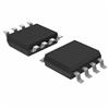
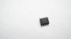
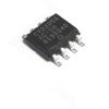
Package / Case
: SOIC-8
Maximum Operating Temperature
: + 70 C
Minimum Operating Temperature
: 0 C
Output Frequency Range
: 10 MHz to 133.3 MHz
Pinout Description
The CY2304SC-2 has two banks of two outputs each.The CY2304 PLL enters a power-down state when there are no rising edges on the REF input. In this mode, all outputs are three-stated and the PLL is turned off, resulting in less than 25 A of current draw.Multiple CY2304 devices can accept the same input clock and distribute it in a system. In this case, the skew between the outputs of two devices is guaranteed to be less than 500 ps.The CY2304 is available in two different configurations, as shown in the "Available Configurations" table. The CY23041 is the base part, where the output frequencies equal the reference if there is no counter in the feedback path.The CY23042 allows the user to obtain Ref and 1/2x or 2x frequencies on each output bank. The exact configuration and output frequencies depends on which output drives the feedback pin.
CY2304SC-2 has many unique features: The first one is multiple configurations.The second one is multiple low-skew outputs.The third one is zero input-output propagation delay, adjustable by capacitive load on FBK input.The forth one is 10-MHz to 133-MHz operating range.The fifth one is low jitter, less than 200 ps cycle-cycle.The sixth one is space-saving 8-pin 150-mil SOIC package.The seventh one is 3.3V operation,etc.
There are some maximum ratings about CY2304SC-2 .Supply voltage to ground potential is -0.5 V to 7.0 V.DC input voltage(excel ref) is -0.5 V to VDD +0.5 V.DC input voltage REF is -0.5 V to 7 V.Storage temperature is -65 to 150.Junction temperature is 150.Otherwise,there are also some electrical charactersitics about it.Input low voltage(VIL) is 0.8 V max.Input high voltage(VIH) is 2.0 V min.Input low current(IIL) is 50.0 uA max when Vin is 0 V.Input high current(IIH) is 100.0 uA max when Vin is VDD.
 CY2304SC-2 Data Sheet