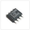
Features: • 335 ps max Total Timing Budget™ (TTB)™ window• 2.5V or 3.3V outputs• 20 LVCMOS outputs• 50 MHz to 200 MHz output frequency• 50 MHz to 200 MHz input frequency• Integrated phase-locked loop (PLL) with lock indicator• Spread Aware͐...
CY23020-1: Features: • 335 ps max Total Timing Budget™ (TTB)™ window• 2.5V or 3.3V outputs• 20 LVCMOS outputs• 50 MHz to 200 MHz output frequency• 50 MHz to 200 MHz in...
SeekIC Buyer Protection PLUS - newly updated for 2013!
268 Transactions
All payment methods are secure and covered by SeekIC Buyer Protection PLUS.
Parameter | Description | Test Conditions | Unit |
VDD | Voltage on any VDD pin with respect to GND | 0.5 to +5 | V |
VIN | Voltage on any input pin with respect to GND | 0.5 to VDD + 0.5 | V |
TSTG | Storage Temperature | 65 to +150 | °C |
TA | Operation Temperature (TSSOP) | 0 to +70 | °C |
Operation Temperature (QFN) | 40 to +85 | °C | |
TJ | Junction Temperature | +150 max | °C |
PD | Package Power Dissipation (TSSOP) | 1 | W |
The CY23020-1-1 is a high-performance 200-MHz PLL-based zero delay buffer designed for high-speed clock distribution applications. The device features a guaranteed TTB window specifying all occurrences of output clocks with respect to the input reference clock across variations in output frequency, supply voltage, operating temperature, input edge rate, and process.
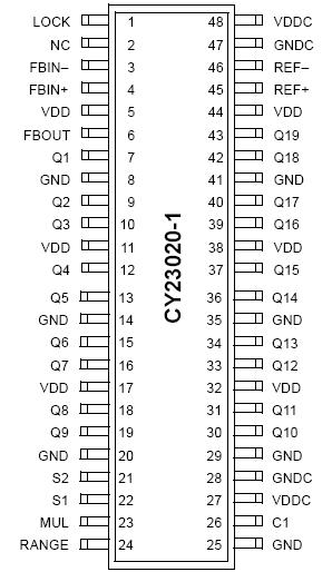
The CY23020-1 outputs are three-state when S1 = S2 = 0 for reduced power. When S1 = 1 and S2 = 0 the PLL is bypassed and the CY23020-1 functions as a fan-out buffer.