Features: • Mixed 2.5V and 3.3V operation
• Complete clock solution for Pentium® /II, Cyrix 6x86,and AMD K6 processor-based motherboards
-Four CPU clocks at 2.5V or 3.3V
-Twelve 3.3V SDRAM clocks[1]
-Five synchronous PCI clocks, one free-running
-One 3.3V 48 MHz USB clock
-One 3.3V Ref. clock at 14.318 MHz
-Two AGP clocks at 3.3V
• Support for ALI (-1 option) and VIA (-2 option)
• I2C™ Serial Configuration Interface
• Full EMI control with factory-EPROM programmable output drive and slew rate
• Factory-EPROM programmable CPU clock frequencies for custom configurations
• Power-down, CPU stop, and PCI stop pins
• Available in space-saving 48-pin SSOP packagePinout SpecificationsSupply Voltage ..................................................0.5 to +7.0V
Input Voltage .............................................. 0.5V to VDD+0.5
Storage Temperature (Non-Condensing) ... 65°C to +150°C
Max. Soldering Temperature (10 sec) ...................... +260°C
Junction Temperature ............................................... +150°C
Package Power Dissipation .............................................. 1W
Static Discharge Voltage ........................................... >2000VDescriptionThe CY2283 is a clock Synthesizer/Driver for Pentium, Cyrix,or AMD processor-based PCs using the ALI Aladdin V (-1 option) or VIA MVP3 (-2 option) chipset.
The CY2283 outputs four CPU clocks at 2.5V or 3.3V. There are five PCI clocks, running at 30 or 33.3 MHz. One of the PCI clocks is free-running. Additionally, the part outputs twelve 3.3V SDRAM clocks
[1], one 3.3V USB clock at 48 MHz, and one 3.3V reference clock at 14.318 MHz. Finally, the part outputs two AGP clocks running at 66.66 MHz or 60 MHz.
The CY2283 has the flexibility to work as either a one-chip or as part of a two-chip clocking solution. In 100-MHz board designs based on the ALI Aladdin V chipset, it is recommended that the CY2283 be used with an external SDRAM buffer solution such as the CY2318NZ or CY2314NZ. In this configuration the SDRAM outputs on the CY2283 must be either turned off using I2C or left floating. The CY231xNZ family provides theSDRAM outputs in place of the CY2283 and can be placed in close proximity to the SDRAM modules.
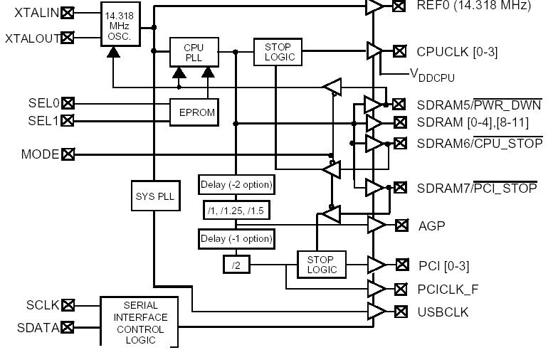
The CY2283 possesses power-down, CPU stop, and PCI stop pins for power management control. These inputs are multiplexed with SDRAM clock outputs, and are selected when the MODE pin is driven LOW. Additionally, the signals are synchronized on-chip, and ensure glitch-free transitions on the outputs.
When the CPU_STOP input is asserted, the CPU clock outputs are driven LOW. When the PCI_STOP input is asserted, the PCI clock outputs (except the free-running PCI clock) are driven LOW. When the PWR_DWN pin is asserted, the reference oscillator and PLLs are shut down, and all outputs are driven LOW.
The CY2283 outputs are designed for low EMI emissions. Controlled rise and fall times, unique output driver circuits and factory-EPROM programmable output drive and slew-rate enable optimal configurations for EMI control.

 CY2283 Data Sheet


