CY22150

Features: • Integrated phase-locked loop (PLL)• Commercial and industrial operation• Flash-programmable• Field-programmable• 2-wire serial programming interface• Low-skew, low-jitter, high-accuracy outputs• 3.3V operation with 2.5V output option• 16-...

product image

CY22150 Picture
SeekIC No. : 004319112 Detail

CY22150: Features: • Integrated phase-locked loop (PLL)• Commercial and industrial operation• Flash-programmable• Field-programmable• 2-wire serial programming interface• ...

floor Price/Ceiling Price

Part Number:
CY22150
Supply Ability:
5000

Price Break

  • Qty
  • 1~5000
  • Unit Price
  • Negotiable
  • Processing time
  • 15 Days
Total Cost: $ 0.00

SeekIC Buyer Protection PLUS - newly updated for 2013!

  • Escrow Protection.
  • Guaranteed refunds.
  • Secure payments.
  • Learn more >>

Month Sales

268 Transactions

Rating

evaluate  (4.8 stars)

Upload time: 2024/11/21

Payment Methods

All payment methods are secure and covered by SeekIC Buyer Protection PLUS.

Notice: When you place an order, your payment is made to SeekIC and not to your seller. SeekIC only pays the seller after confirming you have received your order. We will also never share your payment details with your seller.
Product Details

Description


Features:

• Integrated phase-locked loop (PLL)
• Commercial and industrial operation
• Flash-programmable
• Field-programmable
• 2-wire serial programming interface
• Low-skew, low-jitter, high-accuracy outputs
• 3.3V operation with 2.5V output option
• 16-lead TSSOP


Application

Jitter is defined in many ways including: phase noise,long-term jitter, cycle to cycle jitter, period jitter, absolute jitter,and deterministic. These jitter terms are usually given in terms of rms, peak to peak, or in the case of phase noise dBC/Hz with respect to the fundamental frequency. Power Supply Noise and clock output loading are two major system sources of clock jitter. Power Supply noise can be mitigated by proper power supply decoupling (0.1 µF ceramic cap 0.25") of the clock and ensuring a low impedance ground to the chip. Reducing capacitive clock output loading to a minimum lowers current spikes on the clock edges and thus reduces jitter.
Reducing the total number of active outputs will also reduce jitter in a linear fashion. However, it is better to use two outputs to drive two loads than one output to drive two loads.


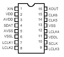
Pinout

  Connection Diagram


Specifications

Parameter Description Min. Max. Unit
VDD Supply Voltage 0.5 7.0 V
VVDDL I/O Supply Voltage 0.5 7.0 V
TS Storage Temperature[3] 65 125 °C
TJ Junction Temperature   125 °C
  Package Power Dissipation-Commercial Temp   450 mW
  Package Power Dissipation-Industrial Temp   380 mW
  Digital Inputs AVSS 0.3 AVDD + 0.3 V
  Digital Outputs referred to VDD AVSS 0.3 AVDD + 0.3 V
  Digital Outputs referred to VDDL AVSS 0.3 VDDL +0.3 V
ESD Static Discharge Voltage per MIL-STD-833, Method 3015   2000 V


Customers Who Bought This Item Also Bought

Margin,quality,low-cost products with low minimum orders. Secure your online payments with SeekIC Buyer Protection.
Batteries, Chargers, Holders
Test Equipment
Sensors, Transducers
Prototyping Products
DE1
Isolators
View more