Features: • An efficient instruction set as a controller - Direct addressing, numerous abbreviated forms, multiplication and division instructions• Instruction sets for C language and RTOS - Highly quadratic instruction system, generalpurpose register of eigth 16-bit ´ 16-bank co...
CXP921064A: Features: • An efficient instruction set as a controller - Direct addressing, numerous abbreviated forms, multiplication and division instructions• Instruction sets for C language and RT...
SeekIC Buyer Protection PLUS - newly updated for 2013!
268 Transactions
All payment methods are secure and covered by SeekIC Buyer Protection PLUS.
• An efficient instruction set as a controller
- Direct addressing, numerous abbreviated forms, multiplication and division instructions
• Instruction sets for C language and RTOS
- Highly quadratic instruction system, generalpurpose register of eigth 16-bit ´ 16-bank configuration
• Minimum instruction cycle :100ns at 20MHz operation (2.7 to 3.3V) 61s at 32kMHz operation (2.2 to 3.3V)
• Incorporated ROM capacity :256K bytes
• Incorporated RAM capacity: 10K bytes
• Peripheral functions
- A/D converter :8-bit 12 analog input, 2 channels successive approximation system, automatic scanning function, (Conversion time: 3.4s at 20MHz)
- Serial interface:128 -byte buffer RAM, 3 channels 8-stage FIFO, 1 channel (supports special mode master/slave)
- I2C bus interface: 64-byte buffer RAM , 2 channels (supports master/slave and automatic transfer mode)
- Timers :8-bit timer/counter, 2 channels (with timing output) 16-bit timer, 3 channels
- Real-time pulse generator :5-bit output, 1 channel (2-stage FIFO)
- Clock prescaler
- Remote control receive circuit :8-bit pulse measurement counter, 8-stage FIFO
• Interruption :30 factors, 30 vectors, multi-interruption and priority selection possible
• Standby mode :Sleep/stop
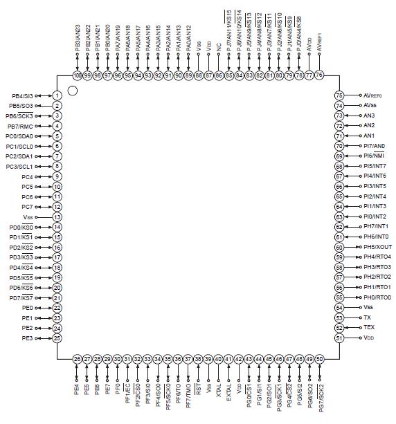
• Package :100-pin plastic QFP/LQFP 104-pin plastic LFLGA
• Piggy/evaluation chip: CXP921000A
• FLASH EEPROM incorporated version :CXP921F064A
Item | Symbol | Rating | Unit | Remarks |
Supply voltage |
VDD | 0.3 to +4.6 | V | |
AVDD | AVss to +4.6*1 | V | ||
AVSS | 0.3 to +0.3 | V | ||
Input voltage | VIN | 0.3 to +4.6*2 | V | |
Output voltage | VOUT | 0.3 to +4.6*2 | V | |
High level output current | IOH | -5 | mA | Output (value per pin) |
High level total output current | IOH | -50 | mA | Total for all output pins |
Low level output current | IOL | 15 | mA | All pins excluding large current output pins(value per pin) |
CIOL | 20 | mA | Large current output pins*3(value per pin) | |
Low level total output current | IOL | 130 | mA | Total for all output pins |
Operating temperature | Topr | 20 to +75 | °C | |
Storage temperature | Tstg | 55 to +150 | °C | |
Allowable power dissipation | PD | 600 | mW | QFP-100P-L01 |
38 | LQFP-100P-L01 | |||
500 | LFLGA-104P-02 |