Features: • A wide instruction set (213 instructions) which covers various types of data
- 16-bit arithmetic instruction/multiplication and division instruction/boolean bit operation instruction
• Minimum instruction cycle During operation 333ns/12MHz (3.0 to 5.5V) During operation 250ns/16MHz (4.5 to 5.5V) During operation 122µs/32kHz
• Incorporated PROM capacity 48 Kbytes
• Incorporated RAM capacity 1376 bytes
• Peripheral functions
- A/D converter 8 bit, 12-channel, successive approximation system (Conversion time 20.0µs/16MHz)
- Serial interface Incorporated buffer RAM (1 to 32 bytes auto transfer) 1-channel Incorporated 8-bit and 8-stage FIFO (1 to 8 bytes auto transfer) 1-channel
- Timer 8-bit timer 8-bit timer/counter 19-bit time base timer 32kHz timer/counter
- High precision timing pattern generator PPG 19-pin 32-stage programmable RTG 5-pin, 2-channel
- PWM/DA gate output PWM 12-bit, 2-channel (Repetitive frequency 62kHz/16MHz) DA gate pulse output 13-bit, 4-channel
- Servo input control Capstan FG, Drum FG/PG, CTL input
- VSYNC separator
- FRC capture unit Incorporated 26-bit and 8-stage FIFO
- PWM output 14-bit, 1-channel
- VISS/VASS circuit Pulse duty auto detection circuit
- Remote control receiving circuit 8-bit pulse measuring counter, 6-stage FIFO
- General purpose prescaler 7-bit (SYNC1 input frequency divided, FRC capture possible)
- HSYNC counter 12-bit event counter (counts SYNC1 input)
• Interruption 22 factors, 15 vectors, multi-interruption possible
• Standby mode SLEEP/STOP
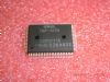
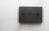
• Package 100-pin plastic QFP/LQFPPinout Specifications
| Item |
Symbol |
Rating |
Unit |
Remarks |
| Supply voltage |
VDD |
0.3 to +7.0 |
V |
|
| VPP |
0.3 to +13 |
V |
Unique to version with incorporated PROM |
| AVDD |
AVss to +7.0*1 |
V |
|
| AVSS |
0.3 to +0.3 |
V |
|
| Input voltage |
VIN |
0.3 to +7.0*2 |
V |
|
| Output voltage |
VOUT |
0.3 to +7.0*2 |
V |
|
| Mid-voltage drive output voltage |
VOUTP |
0.3 to +15.0 |
V |
PH pin |
| High level output current |
IOH |
5 |
mA |
|
| High level total output current |
IOH |
50 |
mA |
Total of all output pins |
| Low level output current |
IOL |
15 |
mA |
Ports excluding large current output
(value per pin) |
| IOLC |
20 |
mA |
High current port output pin*3: per pin |
| Low level total output current |
IOL |
130 |
mA |
Total for all outputs |
| Operating temperature |
Topr |
20 to +75 |
°C |
|
| Storage temperature |
Tstg |
55 to +150 |
°C |
|
| Allowable power dissipation |
PD |
600 |
|
QFP package type |
| 380 |
mW |
LQFP package type |
DescriptionThe CXP872P48A is a CMOS 8-bit microcomputer which consists of A/D converter, serial interface,timer/counter, time base timer, vector interruption,high precision timing pattern generation circuit, PWM generator, PWM for tuner, VISS/VASS circuit, 32kHz timer/event counter, remote control receiving circuit,general purpose prescaler, HSYNC counter, VCR
vertical sync separation circuit and the measuring circuit which measure signals of capstan FG and drum FG/PG and other servo systems, as well as basic configurations like 8-bit CPU, PROM, RAM and I/O port. They are integrated into a single chip.
Also this IC provides sleep/stop function which enables to lower power consumption and ultra-low speed instruction mode in 32kHz operation.
The CXP872P48A is the on-chip PROM version of the CXP87248A with on-chip mask ROM, providing the function of being able to write directly into the program. It is suitable for evaluation use during system development and for small quantity production.

 CXP872P48A Data Sheet