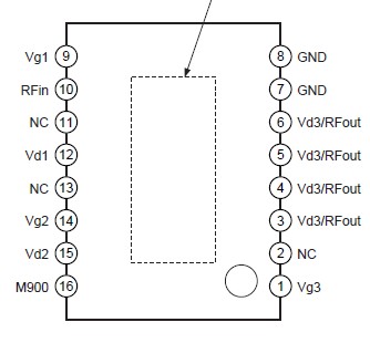
Features: • Single positive rail only• Typical output power of 35.5dBm at 900MHz and 33dBm at 1800MHz• Typical efficiency of 37% at 900MHz and 37% at 1800MHz• Small package size with integral heat-sink: 16-pin HSOF (5.6 ´ 4.4 ´ 0.9mm)• 3-stage amplifier ch...
CXG1047FN: Features: • Single positive rail only• Typical output power of 35.5dBm at 900MHz and 33dBm at 1800MHz• Typical efficiency of 37% at 900MHz and 37% at 1800MHz• Small package s...
SeekIC Buyer Protection PLUS - newly updated for 2013!
268 Transactions
All payment methods are secure and covered by SeekIC Buyer Protection PLUS.
Drain voltage |
VDD1, VDD2, VDD3 |
8 |
V |
Gate voltage |
VGG1, VGG2, VGG3 |
5 to +1 |
V |
Input power |
Pin, max. |
12 |
dBm |
Channel temperature |
Tch, max. |
150 |
°C |
Operating temperature |
Ta |
30 to +90 |
°C |
Storage temperature |
Tstg |
40 to +150 |
°C |
The CXG1047FN dual band GaAs PA is a 3-stage power amplifier that may be used for both GSM900 and DCS1800 applications. To achieve minimum die-size and package dimensions, it contains one amplifier chain with a single input and output.
The CXG1047FN has a single RF input for both the GSM900 and DCS1800 transmit signals. The amplifier can be configured for 2 separate inputs. Power control is best achieved by variation of VDD1/VDD2 and VDD3 drain voltages with an external transistor. A proposed power control circuit configuration is described. External PMOS drain switch should be used to achieve low leakage.