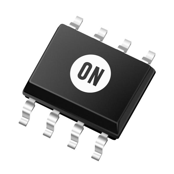
CS81

Features: • Technology : 0.18 m silicon-gate CMOS, 3- to 5-layer wiring capable of integrating a mixture of highspeed processes and cells on a single chip (under development)• Supply voltage : +1.8 V ± 0.15 V (typical) to +1.1 V ± 0.1 V• Junction temperature range : -40 to +125 °...

product image

CS81 Picture
SeekIC No. : 004316734 Detail

CS81: Features: • Technology : 0.18 m silicon-gate CMOS, 3- to 5-layer wiring capable of integrating a mixture of highspeed processes and cells on a single chip (under development)• Supply vol...

floor Price/Ceiling Price

Part Number:
CS81
Supply Ability:
5000

Price Break

  • Qty
  • 1~5000
  • Unit Price
  • Negotiable
  • Processing time
  • 15 Days
Total Cost: $ 0.00

SeekIC Buyer Protection PLUS - newly updated for 2013!

  • Escrow Protection.
  • Guaranteed refunds.
  • Secure payments.
  • Learn more >>

Month Sales

268 Transactions

Rating

evaluate  (4.8 stars)

Upload time: 2024/12/21

Payment Methods

All payment methods are secure and covered by SeekIC Buyer Protection PLUS.

Notice: When you place an order, your payment is made to SeekIC and not to your seller. SeekIC only pays the seller after confirming you have received your order. We will also never share your payment details with your seller.
Product Details

Description


Features:

• Technology : 0.18 m silicon-gate CMOS, 3- to 5-layer wiring capable of integrating a mixture of highspeed processes and cells on a single chip (under development)
• Supply voltage : +1.8 V ± 0.15 V (typical) to +1.1 V ± 0.1 V
• Junction temperature range : -40 to +125 °C (standard specification)
• Gate delay time : tpd = 11 ps (1.8 V, inverter, F/O = 1)
• Gate power consumption : 5 nW/MHz/BC (1.1 V, 2-NAND, F/O = 1)
• High-load drive capability : IOL = 2/4/8/12 mA mixable
• Output buffer cells with noise reduction circuits
• Inputs with on-chip input pull-up/pull-down resistors (33 kW typical) and bidirectional buffer cells
• Buffer cell dedicated to crystal oscillator
• Special interfaces (P-CML, LVDS, PCI, AGP, USB, SDRAM-I/F, SSTL, etc. under development)
• IP macros (CPU, DSP, PCI, IEEE1394, USB, IrDA, PLL, ADC, DAC, etc. under development)
• Capable of incorporating compiled cells (RAM/ROM/multiplier, etc.)
• Configurable internal bus circuits
• Advanced hardware/software co-design environment
• Short-term development using a timing driven layout tool
• Support for static timing sign-off Dramatically reducing the time for generating test vectors for timing verification and the simulation time
• Hierarchical design environment for supporting large-scale circuits
• Simulation (before layout) considering the input slew rate and detailed RC delay calculation (after layout) , supporting development with minimized timing trouble after trial manufacture
• Support for memory (RAM/ROM) SCAN
• Support for memory (RAM) BIST
• Support for boundary SCAN
• Support for path delay test
• A variety of package options (TQFP, HQFP, EBGA, FBGA, TAB-BGA, FCBGA)


Specifications

Parameter
Symbol
Application
Value
Unit
Min.
Max.
Power supply voltage
VDD
VDD, VDDI (Internal)
VDDE (External)
VSS - 0.5
VSS - 0.5
+2.5
+4.0
V
V
Input voltage*1
VI
1.8 V input pin
3.3 V input pin
VSS - 0.5
VSS - 0.5
VDDI + 0.5
( 2.5 V)
VDDE + 0.5
(4.0 V)
V
V
Output voltage
VO
1.8 V output pin
3.3 V output pin
VSS - 0.5
VSS - 0.5
VDDI + 0.5
( 2.5 V)
VDDE + 0.5
( 4.0 V)
V
V
Storage temperature

TST
Plastic package
-55
+125
°C
Power-supply pin current *2
ID
Per VDD/VDDI/VDDE pin
Per VSS pin
-
-
TBD
TBD
mA
mA
Output current*3
IO
L type output buffer IOL = 2 mA
M type output bufferIOL = 4 mA
H type output buffer IOL = 8 mA
V type output buffer IOL = 12 mA
-
-
-
-
±13
±13
±13
±26
mA
mA
mA
mA

*1 : Do not apply any voltage of 1.1 V or more between the LVDS (resistor built-in type) differential inputs.
*2 : Maximum supply current which can be supplied constantly.
*3 : Maximum output current which can be supplied constantly. Exceeding the rating is allowed only within 1 second for only one LSI pin. The maximum rating of the P-CML output buffer is 20 mA.

WARNING: Semiconductor devices can be permanently damaged by application of stress (voltage, current, temperature, etc.) in excess of absolute maximum ratings. Do not exceed these ratings.


Description

The CS81 series of 0.18 m CMOS standard cell arrays is a line of highly integrated CMOS ASICs featuring high speed and low power consumption at the same time.

This series CS81 incorporates up to 40 million gates which have a gate delay time of 11 ps, resulting in both integration and speed about three times higher than conventional products.

In addition, this series CS81 can operate at a power-supply voltage of up to 1.1 V, substantially reducing power consumption.


Customers Who Bought This Item Also Bought

Margin,quality,low-cost products with low minimum orders. Secure your online payments with SeekIC Buyer Protection.
Hardware, Fasteners, Accessories
Crystals and Oscillators
Sensors, Transducers
Prototyping Products
DE1
Programmers, Development Systems
Industrial Controls, Meters
View more