Pinout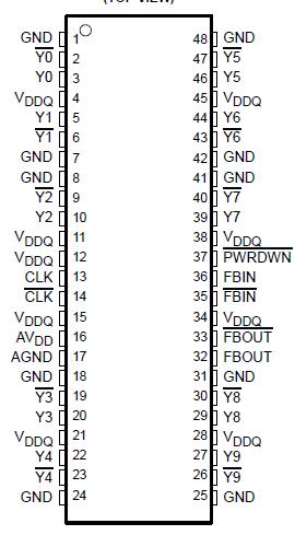 Specifications
Supply voltage range, VDDQ, AVDD . . . . . . . . . . . . . . . . . . . . . . . . . 0.5 V to 3.6 V
Input voltage range, VI (see Notes 1 and 2) . . . . . . . . . . . . .. 0.5 V to VDDQ 0.5
Output voltage range, VO (see Notes 1 and 2) . . . . . . . . . . 0.5 V to VDDQ 0.5 V
Input clamp current, IIK (VI < 0 or VI > VDDQ) . . . . . . . . . . . . . . . . . . . . . . ±50 mA
Output clamp current, IOK (VO < 0 or VO > VDDQ) . . . . . . . . . . . . . . . . . . . ±50 mA
Continuous output current, IO (VO = 0 to VDDQ) . . . . . . . . . . . . . . . . . . . . ±50 mA
Continuous current to GND or VDDQ . . . . . . . . . . . . . . . . . . . . . . . . . . . . . ±100 mA
Package thermal impedance, JA (see Note 3): DGG package . . . . . . .. . . 89°C/W
GQL package . . . . . . . . . . . . . . . . . . . . . . . . . . . . . . . . . . . . . . . . . . . . . 137.6°C/W
Storage temperature range Tstg . . . . . . . . . . . . . . . . . . . . . . . . . . 65°C to 150°C
DescriptionThe CDCV857A is a high-performance, low-skew, low-jitter zero delay buffer that distributes a differential clock input pair (CLK, CLK) to ten differential pairs of clock outputs (Y[0:9], Y[0:9]) and one differential pair of feedback clock output (FBOUT, FBOUT). The clock outputs are controlled by the clock inputs (CLK, CLK), the feedback clocks (FBIN, FBIN), and the analog power input (AVDD). When PWRDWN is high, the outputs switch in phase and frequency with CLK. When PWRDWN is low, all outputs are disabled to high impedance state (3-state), and the PLL is shut down (low power mode). The device also enters this ow power mode when the input frequency falls below a suggested detection frequency that is below 20 MHz (typical 10 MHz). An input frequency detection circuit will detect the low frequency condition and after applying a >20 MHz input signal this detection circuit turns on the PLL again and enables the outputs.
When AVDD is strapped low, the PLL is turned off and bypassed for test purposes. The CDCV857A is also able to track spread spectrum clocking for reduced EMI.
Since the CDCV857A is based on PLL circuitry, it requires a stabilization time to achieve phase-lock of the PLL. This stabilization time is required following power up. The CDCV857A is characterized for operation from 0°C to 85°C.

 CDCV857A Data Sheet