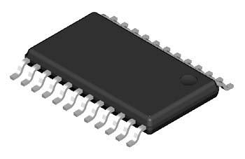
Pinout Description
The CDCF5801A provides clock multiplication from a reference clock (REFCLK) signal with the unique capability to delay or advance the CLKOUT/CLKOUTB with steps of only 1.3 mUI through a phase aligner. For every rising edge on the DLYCTRL pin the CLKOUT is delayed by a 1.3-mUI step size as long as the LEADLAG input detects a low signal at the time of the DLYCTRL rising edge. Similarly for every rising edge on the DLYCTRL pin the CLKOUT is advanced by a 1.3-mUI step size as long as the LEADLAG pin is high during the transition. This unique capability allows the device to phase align (zero delay) between CLKOUT/CLKOUTB and any one other CLK in the system by feeding the clocks that need to be aligned to the DLYCTRL and the LEADLAG pins.
Features of the CDCF5801A are:(1)Low-Jitter Clock Multiplier: × 1, × 2, × 4, × 8; (2)Fail-Safe Power Up Initialization; (3)Programmable Bidirectional Delay Steps of 1.3 mUI; (4)Output Frequency Range of 25 MHz to 280 MHz; (5)Input Frequency Range of 12.5 MHz to 240 MHz; (6)Low Jitter Generation; (7)Single-Ended REFCLK Input With Adjustable Trigger Level (Works With LVTTL, HSTL, and LVPECL); (8)Differential/Single-Ended Output; (9)Output Can Drive LVPECL, LVDS, and LVTTL; (10)Three Power Operating Modes to Minimize Power; (11)Low Power Consumption ( < 190 mW at 280 MHz/3.3 V); (12)Packaged in a Shrink Small-Outline Package(DBQ); (13)No External Components Required for PLL; (14)Spread Spectrum Clock Tracking Ability to Reduce EMI (SSC).
The absolute maximum ratings of the CDCF5801A can be summarized as:(1)Supply voltage range -0.5 V to 4 V; (2)Voltage range at any output terminal -0.5 V to V DD + 0.5 V; (3)Voltage range at any input terminal -0.5 V to V DD + 0.5 V; (4)Storage temperature range -65 ° C to 150 ° C; (5)Lead temperature 1,6 mm (1/16 inch) from case for 10 seconds 260 ° C.
If you want to know more CDCF5801A information such as the electrical characteristics ,please download the datasheet in www.seekdatasheet.com .

 CDCF5801A Data Sheet


