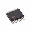
Pinout Description
The CDCE72010 is a high-performance, low phase noise, and low skew clock synchronizer that synchronizes a VCXO (Voltage Controlled Crystal Oscillator) or VCO (Voltage Controlled Oscillator) frequency to one of two reference clocks. The clock path is fully programmable providing the user with a high degree of flexibility. The following relationship applies to the dividers:Frequency (VCXO_IN or AUX_IN) / Frequency (PRI_REF or SEC_REF) = (P*N)/(R*M) The VC(X)O_IN clock operates up to 1.5GHz through the selection of external VC(X)O and loop filter components. The PLL loop bandwidth and damping factor can be adjusted to meet different system requirements.
Features of the CDCE72010 are:(1)High Performance LVPECL, LVDS, LVCMOS PLL Clock Synchronizer; (2)Two Reference Clock Inputs (Primary and Secondary Clock) for Redundancy Support with Manual or Automatic Selection; (3)Accepts Two Differential Input (LVPECL or LVDS) References up to 500MHz (or Two LVCMOS Inputs up to 250MHz) as PLL Reference; (4)VCXO_IN Clock is Synchronized to One of Two Reference Clocks; (5)VCXO_IN Frequencies up to 1.5GHz (LVPECL) 800Mhz for LVDS and 250MHz for LVCMOS Level Signaling; (6)Outputs Can be a Combination of LVPECL,LVDS, and LVCMOS (Up to 10 Differential LVPECL or LVDS Outputs or up to 20 LVCMOS Outputs), Output 9 can be Converted to an Auxiliary Input as a 2nd VC(X)O.
The absolute maximum ratings of the CDCE72010 can be summarized as:(1)Supply voltage range (1): 0.5 ~4.6 V; (2)Input voltage range (2): 0.5 V CC + 0.5 V; (3)Output voltage range (2): 0.5 V CC + 0.5 V; (4)Input current V I < 0, V I > V CC :± 20 mA; (5)Output current for LVPECL/LVCMOS Outputs 0 < V O < V CC:± 50 mA; (6)Junction temperature :125 ° C; (7)Storage temperature range: 65~ 150 ° C.
If you want to know more CDCE72010 information such as the electrical characteristics ,please download the datasheet in www.seekdatasheet.com .

 CDCE72010 Data Sheet


