CDC9842

Features: Provides System Clock Solution for PentiumTM/82430X/82430VX and PentiumPro 82440FX ChipsetsFour Host-Clock Outputs With Programmable Frequency (50 MHz, 60 MHz and 66 MHz)Six PCI Clock Outputs at Half-CPU FrequencyOne 48-MHz Universal Serial Bus (USB) Clock OutputThree 14.318-MHz Referenc...

product image

CDC9842 Picture
SeekIC No. : 004312271 Detail

CDC9842: Features: Provides System Clock Solution for PentiumTM/82430X/82430VX and PentiumPro 82440FX ChipsetsFour Host-Clock Outputs With Programmable Frequency (50 MHz, 60 MHz and 66 MHz)Six PCI Clock Outp...

floor Price/Ceiling Price

Part Number:
CDC9842
Supply Ability:
5000

Price Break

  • Qty
  • 1~5000
  • Unit Price
  • Negotiable
  • Processing time
  • 15 Days
Total Cost: $ 0.00

SeekIC Buyer Protection PLUS - newly updated for 2013!

  • Escrow Protection.
  • Guaranteed refunds.
  • Secure payments.
  • Learn more >>

Month Sales

268 Transactions

Rating

evaluate  (4.8 stars)

Upload time: 2024/11/21

Payment Methods

All payment methods are secure and covered by SeekIC Buyer Protection PLUS.

Notice: When you place an order, your payment is made to SeekIC and not to your seller. SeekIC only pays the seller after confirming you have received your order. We will also never share your payment details with your seller.
Product Details

Description


Features:

 Provides System Clock Solution for PentiumTM/82430X/82430VX and PentiumPro 82440FX Chipsets
 Four Host-Clock Outputs With Programmable Frequency (50 MHz, 60 MHz and 66 MHz)
 Six PCI Clock Outputs at Half-CPU Frequency
 One 48-MHz Universal Serial Bus (USB) Clock Output
 Three 14.318-MHz Reference Clock Outputs
 All Output Clock Frequencies Derived From a Single 14.31818-MHz Crystal Input
 LVTTL-Compatible Inputs and Outputs
 Internal Loop Filters for Phase-Locked Loops Eliminate the Need for External Components
 Operates at 3.3 VCC
Packaged in Plastic Small-Outline Package


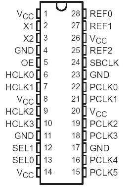
Pinout

  Connection Diagram


Specifications

Supply voltage range, VCC . . . . . . . . . . . . . . . . . . . . . . . . . . . . . . . . . . . . . .  . .0.5 V to 4.6 V
Input voltage range, VI . . . . . . . . . . . . . . . . . . . . . . . . . . . . . . . . . . . . . . . . . . .0.5 V to 4.6 V
Voltage range applied to any output in the high-impedance state or power-off state,
     VO (see Note 1)  . . . . . . . . . . . . . . . . . . . . . . . . . . . . . . . . . . . . .. . . .0.5 V to VCC + 0.5 V
Current into any output in the low state, IO  . . . . . . . . . . . . . . . . . . . . . . . . . . . . . . . . . .16 mA
Input clamp current, IIK (VI < 0) . . . . . . . . . . . . . . . . . . . . . . . . . . . . . . . . . . . .  . . . . . .18 mA
Output clamp current, IOK (VO < 0)  . . . . . . . . . . . . . . . . . . . . . . . . . . . . . . . . . . . . . . . .50 mA
Maximum power dissipation at TA = 55°C (in still air) (see Note 2)  . . . . . . . . . . . . . . . . .1.2 W
Storage temperature range, Tstg  . . . . . . . . . . . . . . . . . . . . . . . . . . . . . . . . . . .65°C to 150°C


Description

The CDC9842 is a high-performance clock synthesizer/driver that generates the system clocks necessary to support PentiumE/82430X/82430VX and PentiumPro 82440FX chipsets. Four host-clock outputs (HCLKn) are programmable to one of three frequencies (50 MHz, 60 MHz, or 66 MHz) via the SEL0 and SEL1 control inputs. Six PCI-clock outputs (PCLKn) are half the frequency of CPU clock outputs and are delayed 1 ns to 4 ns from the rising edge of the CPU clock. In addition, a universal serial bus (USB) clock output at 48 MHz (SBCLK) and three 14.318-MHz reference clock outputs (REF0, REF1, REF2) are provided.

All CDC9842 output frequencies are generated from a 14.318-MHZ crystal input. A reference clock can be provided at the X1 input instead of a crystal input.

Two phase-locked loops (PLLs) CDC9842 are used to generate the host clock frequency and the 48-MHz clock frequency. On-chip loop filters and internal feedback eliminate the need for external components. The PCI-clock frequency is derived directly from the host-clock frequency. The PLL circuit can be bypassed in the TEST mode (i.e., SEL0 = SEL1 = H) to distribute a test clock provided at the X1 input.

The host- and PCI-clock outputs CDC9842 provide low-skew/low-jitter clock signals for reliable clock operation. All outputs are 3 state and are enabled via OE.

Because the CDC9842 is based on PLL circuitry, it requires a stabilization time to achieve phase-lock of the PLL. This stabilization time is required following power up and application of a fixed-frequency, fixed-phase signal at the X1 input, as well as following any changes to the OE or SELn inputs.


Customers Who Bought This Item Also Bought

Margin,quality,low-cost products with low minimum orders. Secure your online payments with SeekIC Buyer Protection.
Cables, Wires - Management
Prototyping Products
DE1
Connectors, Interconnects
Tapes, Adhesives
803
Test Equipment
View more