CDC9841

Features: Four CPU Clock Outputs With Programmable Frequency (50 MHz, 60 MHz, and 66 MHz)Six Clock Outputs at Half-CPU Frequency for PCIOne 24-MHz Clock OutputOne 12-MHz Clock OutputTwo 14.318-MHz Reference OutputsAll Output Clock Frequencies Derived From a Single 14.31818-MHz Crystal Input LVTTL-...

product image

CDC9841 Picture
SeekIC No. : 004312270 Detail

CDC9841: Features: Four CPU Clock Outputs With Programmable Frequency (50 MHz, 60 MHz, and 66 MHz)Six Clock Outputs at Half-CPU Frequency for PCIOne 24-MHz Clock OutputOne 12-MHz Clock OutputTwo 14.318-MHz R...

floor Price/Ceiling Price

Part Number:
CDC9841
Supply Ability:
5000

Price Break

  • Qty
  • 1~5000
  • Unit Price
  • Negotiable
  • Processing time
  • 15 Days
Total Cost: $ 0.00

SeekIC Buyer Protection PLUS - newly updated for 2013!

  • Escrow Protection.
  • Guaranteed refunds.
  • Secure payments.
  • Learn more >>

Month Sales

268 Transactions

Rating

evaluate  (4.8 stars)

Upload time: 2024/5/20

Payment Methods

All payment methods are secure and covered by SeekIC Buyer Protection PLUS.

Notice: When you place an order, your payment is made to SeekIC and not to your seller. SeekIC only pays the seller after confirming you have received your order. We will also never share your payment details with your seller.
Product Details

Description


Features:

 Four CPU Clock Outputs With Programmable Frequency (50 MHz, 60 MHz, and 66 MHz)
 Six Clock Outputs at Half-CPU Frequency for PCI
 One 24-MHz Clock Output
 One 12-MHz Clock Output
 Two 14.318-MHz Reference Outputs
 All Output Clock Frequencies Derived From a Single 14.31818-MHz Crystal Input
LVTTL-Compatible Inputs and Outputs
 Internal Loop Filters for Phase-Lock Loops Eliminate the Need for External Components
 Operates at 3.3 VCC
 Distributed VCC and Ground Pins Reduce Switching Noise
 Packaged in Plastic Small-Outline Package


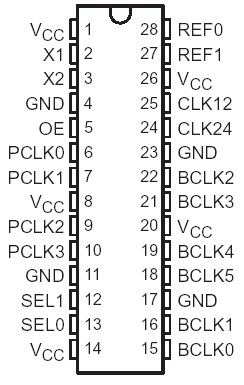
Pinout

  Connection Diagram


Specifications

Supply voltage range, VCC . . . . . . . . . . . . . . . . . . . . . . . . . . . . . . . . . . . . . . . . . . . . . . . . .. .0.5 V to 4.6 V
Input voltage range, VI (see Note 1) . . . . . . . . . . . . . . . . . . . . . . . . . . . . . . . . . . .. . . . . . . .0.5 V to 4.6 V
Voltage range applied to any output in the high state or power-off state,
    VO (see Note 1)  . . . . . . . . . . . . . . . . . . . . . . . . . . . . . . . . . . . . . . . . . . . . . . . . .  . .0.5 V to VCC + 0.5 V
Current into any output in the low state, IO. . . . . . . . . . . . . . . . . . . . . . . . . . . . . . . . . .. . . . . . 2 x IOHmax
Input clamp current, IIK (VI < 0) . . . . . . . . . . . . . . . . . . . . . . . . . . . . . . . . . . . . . . . . . . . . . . . .  . . . .18 mA
Output clamp current, IOK (VO < 0)  . . . . . . . . . . . . . . . . . . . . . . . . . . . . . . . . . . . . . . . . . . . . . . . . . .50 mA
Maximum power dissipation at TA = 55°C (in still air) (see Note 2)  . . . . . . . . . . . . . . . . . . . . . . . . . .  .1.2 W
Storage temperature range, Tstg  . . . . . . . . . . . . . . . . . . . . . . . . . . . . . . . . . . . . . . . . . . . . .65°C to 150°C


Description

The CDC9841 is a high-performance clock synthesizer/driver that generates all required clock signals necessary for a high-performance PC motherboard. The four central processing unit (CPU) clock outputs (PCLKn) are programmable to one of three frequencies (50 MHz, 60 MHz, or 66 MHz) via the SEL0 and SEL1 control inputs. The six peripheral-component-interconnect (PCI) clock outputs (BCLKn) are half the frequency of PCLKn and are delayed 1 ns to 4 ns from the rising edge of the CPU clock. In addition, the four fixed-frequency outputs provide a 24-MHz clock (CLK24), a 12-MHz clock (CLK12), and two buffered copies of the 14.318-MHz input reference (REF0, REF1).

The CDC9841 generates all output frequencies from a 14.31818-MHz crystal input. A reference clock can be provided at X1 instead of a crystal input.

Two phase-lock loops (PLLs)CDC9841  generate the CPU clock frequency and the 24-MHz clock frequency. On-chip loop filters and internal feedback eliminate the need for external components. The PCI and 12-MHz clock frequencies are derived from the base CPU and 24-MHz clock frequencies, respectively. The PLL circuit can
be bypassed in the TEST mode (i.e., SEL0 = SEL1 = H) to distribute a test clock provided at the X1 input. Because the CDC9841 is based on PLL circuitry, CDC9841 requires a stabilization time to achieve phase lock of the PLL. This stabilization time is required following power up and application of a fixed-frequency, fixed-phase signal at the X1 input, as well as following any changes to the SELn inputs.

PCLKn and BCLKn provide low-skew/low-jitter clock signals for reliable clock operation. All outputs are 3 state and are enabled via OE.


Customers Who Bought This Item Also Bought

Margin,quality,low-cost products with low minimum orders. Secure your online payments with SeekIC Buyer Protection.
Optoelectronics
Line Protection, Backups
Memory Cards, Modules
Power Supplies - Board Mount
Static Control, ESD, Clean Room Products
Power Supplies - External/Internal (Off-Board)
View more