CDC950

Features: Generates Clocks for Next Generation MicroprocessorsUses a 14.318-MHz Crystal Input to Generate Multiple Output FrequenciesIncludes Spread Spectrum Clocking (SSC), 0.6% Downspread for Reduced EMI With Theoretical EMI of 7 dBPower Management Control TerminalsLow Output Skew and Jitter for...

product image

CDC950 Picture
SeekIC No. : 004312269 Detail

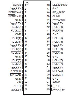
CDC950: Features: Generates Clocks for Next Generation MicroprocessorsUses a 14.318-MHz Crystal Input to Generate Multiple Output FrequenciesIncludes Spread Spectrum Clocking (SSC), 0.6% Downspread for Redu...

floor Price/Ceiling Price

Part Number:
CDC950
Supply Ability:
5000

Price Break

  • Qty
  • 1~5000
  • Unit Price
  • Negotiable
  • Processing time
  • 15 Days
Total Cost: $ 0.00

SeekIC Buyer Protection PLUS - newly updated for 2013!

  • Escrow Protection.
  • Guaranteed refunds.
  • Secure payments.
  • Learn more >>

Month Sales

268 Transactions

Rating

evaluate  (4.8 stars)

Upload time: 2024/5/20

Payment Methods

All payment methods are secure and covered by SeekIC Buyer Protection PLUS.

Notice: When you place an order, your payment is made to SeekIC and not to your seller. SeekIC only pays the seller after confirming you have received your order. We will also never share your payment details with your seller.
Product Details

Description


Features:

 Generates Clocks for Next Generation  Microprocessors
 Uses a 14.318-MHz Crystal Input to Generate Multiple Output Frequencies
 Includes Spread Spectrum Clocking (SSC), 0.6% Downspread for Reduced EMI With Theoretical EMI of 7 dB
 Power Management Control Terminals
 Low Output Skew and Jitter for Clock Distribution
 Operates From a Single 3.3-V Supply
 Generates the Following Clocks:
   − 8 Host (Diff Pairs, 100/133 MHz)
   − 1 CLK33 (3.3 V, 33.3 MHz)
   − 1 REFCLK (3.3 V, 14.318 MHz)
   − 2 3V48 (3.3 V, 180° Shifted Pairs, 48 MHz)
 Packaged in a 48-Pin TSSOP Package


Application

Audio                                www.ti.com/audio
Automotive                       www.ti.com/automotive
Broadband                        www.ti.com/broadband
Digital Control                   www.ti.com/digitalcontrol
Military                              www.ti.com/military
Optical Networking           www.ti.com/opticalnetwork
Security                            www.ti.com/security
Telephony                        www.ti.com/telephony
Video & Imaging               www.ti.com/video
Wireless                           www.ti.com/wireless


Pinout

  Connection Diagram


Specifications

Supply voltage range, VCC . . . . . . . . . . . . . . . . . . . . . . . . . . . . . . . . .  . . . . . . . 0.5 V to 4.6 V
Input voltage range, VI (see Note 1) . . . . . . . . . . . . . . . . . . . . . . . . ..  . . . . . . . . 0.5 V to 7 V
Voltage range applied to any output in the high-impedance
or power-off state, VO (see Note 1) . . . . . . . . . . . . . . .. . . .. . . . . .. . . . . . . . . . . 0.5 V to 7 V
Current into any output in the low state, IO . . .. .. . . . . .  . . . . . . . . . . . . . . . . . . 2 * rated IOL
Input clamp current, IIK (VI < 0) . . . . . . . . . . . . . . . . . . .  . . . . . . . . . . . . . . . . . . . . . . . 50 mA
Output clamp current, IOK (VO < 0) . . . . . . . . . . . . . . . . . . . . . . . . . . . . . . . . . . . . . . . . 50 mA
                                         (VO > VDD) .. . . . . . . . . . . . . . . . . . . . . . . . . . . . . . . . . . . . . . . 50 mA

Package thermal impedance, JA (see Note 2) . . . . . . . . . . . . . . . . . . . . . . . . . . . . . . . 89°C/W
Maximum power dissipation at TA = 55°C (in still air) (see Note 3)  . . . . . . . . . . . . . . 1070 mW
Operating free-air temperature range, TA . .  . . . . . . . . . . . . . . . . . . . . . . . . . . . 0°C to 85°C
Storage temperature range, Tstg . . . .  . . . . . . . . . . . . . . . . . . . . . . . . . . . . . . 65°C to 150°C
Lead temperature 1,6 mm (1/16 inch) from case for 10 seconds . . . . . . . . . . . . . . . . . . . 260°C
† Stresses beyond those listed under "absolute maximum ratings" may cause permanent damage to the device. These are stress ratings only, and functional operation of the device at these or any other conditions beyond those indicated under "recommended operating conditions" is not implied. Exposure to absolute-maximum-rated conditions for extended periods may affect device reliability.
NOTES: 1. The input and output negative-voltage ratings may be exceeded if the input and output clamp-current ratings are observed.
            2. The package thermal impedance is calculated in accordance with EIA/JEDEC Std JESD51, except for the through-hole packages,which use a trace length of zero.
            3. The maximum package power dissipation is calculated using a junction temperature of 150°C and a board trace length of 750 mils.For more information, refer to the Package Thermal Considerations application note in the ABT Advanced BiCMOS Technology Data Book, literature number SCBD002.


Description

The CDC950 is a differential clock synthesizer/driver that generates HCLK/HCLK, CLK33, 3V48, and REFCLK system clock signals to support a computer system with next generation processors and double data rate (DDR) memory subsystems.

All CDC950 output frequencies are generated from a 14.318-MHz crystal input. A reference clock input can be provided at the XIN input instead of a crystal. Two phase-locked loops (PLLs) are used to generate the host requencies and the 48-MHz clock frequencies. On-chip loop filters and internal feedback eliminate the need for external components.


Customers Who Bought This Item Also Bought

Margin,quality,low-cost products with low minimum orders. Secure your online payments with SeekIC Buyer Protection.
Connectors, Interconnects
Discrete Semiconductor Products
Industrial Controls, Meters
Test Equipment
Tapes, Adhesives
803
View more