CDC318

Features: High-Speed, Low-Skew 1-to-18 Clock Buffer for Synchronous DRAM (SDRAM) Clock Buffering ApplicationsOutput Skew, tsk(o), Less Than 250 psPulse Skew, tsk(p), Less Than 650 ps Supports up to Four Unbuffered SDRAM Dual Inline Memory Modules (DIMMs)I2C Serial Interface Provides Individual En...

product image

CDC318 Picture
SeekIC No. : 004312259 Detail

CDC318: Features: High-Speed, Low-Skew 1-to-18 Clock Buffer for Synchronous DRAM (SDRAM) Clock Buffering ApplicationsOutput Skew, tsk(o), Less Than 250 psPulse Skew, tsk(p), Less Than 650 ps Supports up to...

floor Price/Ceiling Price

Part Number:
CDC318
Supply Ability:
5000

Price Break

  • Qty
  • 1~5000
  • Unit Price
  • Negotiable
  • Processing time
  • 15 Days
Total Cost: $ 0.00

SeekIC Buyer Protection PLUS - newly updated for 2013!

  • Escrow Protection.
  • Guaranteed refunds.
  • Secure payments.
  • Learn more >>

Month Sales

268 Transactions

Rating

evaluate  (4.8 stars)

Upload time: 2024/12/21

Payment Methods

All payment methods are secure and covered by SeekIC Buyer Protection PLUS.

Notice: When you place an order, your payment is made to SeekIC and not to your seller. SeekIC only pays the seller after confirming you have received your order. We will also never share your payment details with your seller.
Product Details

Description


Features:

High-Speed, Low-Skew 1-to-18 Clock Buffer for Synchronous DRAM (SDRAM) Clock Buffering Applications
Output Skew, tsk(o), Less Than 250 ps
Pulse Skew, tsk(p), Less Than 650 ps
Supports up to Four Unbuffered SDRAM Dual Inline Memory Modules (DIMMs)
I2C Serial Interface Provides Individual Enable Control for Each Output
Operates at 3.3 V
Distributed VCC and Ground Pins Reduce Switching Noise
ESD Protection Exceeds 2000 V Per MIL-STD-883, Method 3015
Packaged in 48-Pin Shrink Small Outline (DL) Package


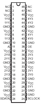
Pinout

  Connection Diagram


Specifications

Supply voltage range, VCC . . . . . . . . . . . . . . . . . . . . . . . . . . . . . . . . . . . . . . . . . . . . . . . . .0.5 V to 4.6 V
Input voltage range, VI (see Note 1) . . . . . . . . . . . . . . . . . . . . . . . . . . . . . . . . . . . . . . . . .0.5 V to 4.6 V
Input voltage range, VI (SCLOCK, SDATA) (see Note 1). . . . . . . . . . . . . . . . . . . . . . . . . . .0.5 V to 6.5 V
Output voltage range, VO (SDATA) (see Note 1) . . . . . . . . . . . . . . . . . . . . . . . . . .. . . . . . .0.5 V to 6.5 V
Voltage range applied to any output in the high or power-off state, VO . . . . . . .. . .0.5 V to VCC +0.5 V
Current into any output in the low state (except SDATA), IO . . . . . . . . . . . . . . . . . . . . . . . . . . . . . .48 mA
Current into SDATA in the low state, IO . . . . . . . . . . . . . . . . . . . . . . . . . . . . . . . . . . . . . . . . . . . . . . .12 mA
Input clamp current, IIK (VI < 0) (SCLOCK) . . . . . . . . . . . . . . . . . . . . . . . . . . . . . . . . . . . . . . . . . . .50 mA
Output clamp current, IOK (VO < 0) (SDATA) . . . . . . . . . . . . . . . . . . . . . . . . . . . . . . . . . . . . . . . . . .50 mA
Package thermal impedance, JA (see Notes 2 and 3) . . . . . . . . . . . . . . . . . . . . . . . . . . . . . . . . . .84°C/W
Storage temperature range, Tstg . . . . . . . . . . . . . . . . . . . . . . . . . . . . . . . . . . . . . . . . . . .65°C to 150°C
Lead temperature 1,6 mm (1/16 inch) from case for 10 seconds . . . . . . . . . . . . . . . . . . . . . . . . . . .260°C


Description

The CDC318 is a high-performance clock buffer that distributes one input (A) to 18 outputs (Y) with minimum skew for clock distribution. The CDC318
operates from a 3.3-V power supply, and is characterized for operation from 0°C to 70°C.

CDC318 provides a standard mode (100K-bits/s) I2C serial interface for device control. The implementation is as a slave/receiver. The device address is specified in the I2C device address table. Both of the I2C inputs (SDATA and SCLOCK) provide integrated pullup resistors (typically 140 k) and are 5-V tolerant.

Three 8-bit I2C registers provide individual enable control for each of the outputs. All CDC318 outputs default to enabled at powerup. Each output can be placed in a disabled mode with a low-level output when a low-level control bit is written to the control register. The CDC318 registers are write only and must be accessed in sequential order (i.e., random access of the registers is not supported).

The CDC318 provides 3-state outputs for testing and debugging purposes. The outputs can be placed in a high-impedance state via the output-enable (OE) input. When OE is high, all outputs are in the operational state. When OE is low, the outputs are placed in a high-impedance state. OE provides an integrated pullup resistor.


Customers Who Bought This Item Also Bought

Margin,quality,low-cost products with low minimum orders. Secure your online payments with SeekIC Buyer Protection.
Memory Cards, Modules
Cables, Wires
Power Supplies - External/Internal (Off-Board)
Discrete Semiconductor Products
RF and RFID
Cable Assemblies
View more