CD74HCT670

Features: • Simultaneous and Independent Read and Write Operations• Expandable to 512 Words of n-Bits• Three-State Outputs• Organized as 4 Words x 4 Bits Wide• Buffered Inputs• Typical Read Time = 16ns for 'HC670 VCC = 5V, CL = 15pF, TA = 25• Fanout (Over ...

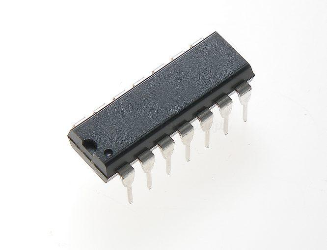
product image

CD74HCT670 Picture
SeekIC No. : 004312184 Detail

CD74HCT670: Features: • Simultaneous and Independent Read and Write Operations• Expandable to 512 Words of n-Bits• Three-State Outputs• Organized as 4 Words x 4 Bits Wide• Buffered...

floor Price/Ceiling Price

Part Number:
CD74HCT670
Supply Ability:
5000

Price Break

  • Qty
  • 1~5000
  • Unit Price
  • Negotiable
  • Processing time
  • 15 Days
Total Cost: $ 0.00

SeekIC Buyer Protection PLUS - newly updated for 2013!

  • Escrow Protection.
  • Guaranteed refunds.
  • Secure payments.
  • Learn more >>

Month Sales

268 Transactions

Rating

evaluate  (4.8 stars)

Upload time: 2024/11/27

Payment Methods

All payment methods are secure and covered by SeekIC Buyer Protection PLUS.

Notice: When you place an order, your payment is made to SeekIC and not to your seller. SeekIC only pays the seller after confirming you have received your order. We will also never share your payment details with your seller.
Product Details

Description


Features:

• Simultaneous and Independent Read and Write Operations
• Expandable to 512 Words of n-Bits
• Three-State Outputs
• Organized as 4 Words x 4 Bits Wide
• Buffered Inputs
• Typical Read Time = 16ns for 'HC670 VCC = 5V, CL = 15pF, TA = 25
• Fanout (Over Temperature Range)
    - Standard Outputs . . . . . . . . . . . . . . . 10 LSTTL Loads
    - Bus Driver Outputs . . . . . . . . . . . . . 15 LSTTL Loads
• Wide Operating Temperature Range . . . -55 to 125
• Balanced Propagation Delay and Transition Times
• Significant Power Reduction Compared to LSTTL Logic ICs
• HC Types
    - 2V to 6V Operation
    - High Noise Immunity: NIL = 30%, NIH = 30% of VCC at VCC = 5V
• HCT Types
    - 4.5V to 5.5V Operation
    - Direct LSTTL Input Logic Compatibility, VIL= 0.8V (Max), VIH = 2V (Min)
    - CMOS Input Compatibility, Il 1mA at VOL, VOH


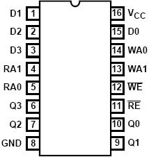
Pinout

  Connection Diagram


Specifications

DC Supply Voltage, VCC . . . . . . . . . . . . . . . . . . . . . . . . . -0.5V to 7V
DC Input Diode Current, IIK
For VI < -0.5V or VI > VCC + 0.5V . . . . . . . . . . . . . . . . . . . . .±20mA
DC Output Diode Current, IOK
For VO < -0.5V or VO > VCC + 0.5V . . . . . . . . . . . . . . . . . . ...±20mA
DC Output Source or Sink Current per Output Pin, IO
For VO > -0.5V or VO < VCC + 0.5V . . . . . . . . . . . . . . . . . . . .±25mA
DC VCC or Ground Current, ICC  . . . . . . . . . . . . . . . . . . . . . . ±50mA


Description

The 'HC670 and CD74HCT670 are 16-bit register files organized as 4 words x 4 bits each. Read and write address and enable inputs allow simultaneous writing into one location while reading another. Four data inputs are provided to store the 4-bit word. The write address inputs (WA0 and WA1) determine the location of the stored word in the register. When write enable (WE) is low the word is entered into the address location and CD74HCT670 remains transparent to the data. CD74HCT670 outputs will reflect the true form of the input data. When (WE) is high data and address inputs are inhibited. Data acquisition from the four registers is made possible by the read address inputs (RA1 and RA0). The addressed word appears at the output when the read enable (RE) is low. CD74HCT670 output is in the high impedance state when the (RE) is high. Outputs can be tied together to increase the word capacity to 512 x 4 bits.


Customers Who Bought This Item Also Bought

Margin,quality,low-cost products with low minimum orders. Secure your online payments with SeekIC Buyer Protection.
Memory Cards, Modules
Inductors, Coils, Chokes
Sensors, Transducers
Transformers
Undefined Category
View more