CD74HCT652

Features: • CD74HC652, CD74HCT652 . . . . . . . . . . . Non-Inverting• Independent Registers for A and B Buses• Three-State Outputs• Drives 15 LSTTL Loads• Typical Propagation Delay = 12ns at VCC = 5V,CL = 15pF• Fanout (Over Temperature Range)- Standard Outputs ...

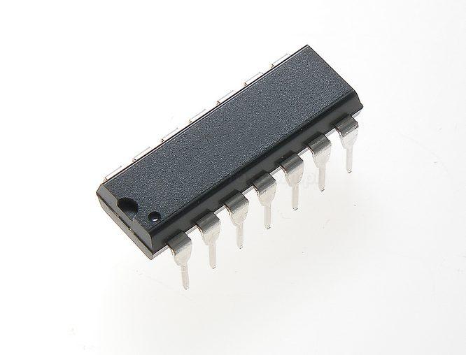
product image

CD74HCT652 Picture
SeekIC No. : 004312183 Detail

CD74HCT652: Features: • CD74HC652, CD74HCT652 . . . . . . . . . . . Non-Inverting• Independent Registers for A and B Buses• Three-State Outputs• Drives 15 LSTTL Loads• Typical Prop...

floor Price/Ceiling Price

Part Number:
CD74HCT652
Supply Ability:
5000

Price Break

  • Qty
  • 1~5000
  • Unit Price
  • Negotiable
  • Processing time
  • 15 Days
Total Cost: $ 0.00

SeekIC Buyer Protection PLUS - newly updated for 2013!

  • Escrow Protection.
  • Guaranteed refunds.
  • Secure payments.
  • Learn more >>

Month Sales

268 Transactions

Rating

evaluate  (4.8 stars)

Upload time: 2024/5/31

Payment Methods

All payment methods are secure and covered by SeekIC Buyer Protection PLUS.

Notice: When you place an order, your payment is made to SeekIC and not to your seller. SeekIC only pays the seller after confirming you have received your order. We will also never share your payment details with your seller.
Product Details

Description


Features:

• CD74HC652, CD74HCT652 . . . . . . . . . . . Non-Inverting
• Independent Registers for A and B Buses
• Three-State Outputs
• Drives 15 LSTTL Loads
• Typical Propagation Delay = 12ns at VCC = 5V,CL = 15pF
• Fanout (Over Temperature Range)
- Standard Outputs . . . . . . . . . . . . . . . 10 LSTTL Loads
- Bus Driver Outputs . . . . . . . . . . . . . 15 LSTTL Loads
• Wide Operating Temperature Range . . . -55oC to 125oC
• Balanced Propagation Delay and Transition Times
• Significant Power Reduction Compared to LSTTL Logic ICs
• Alternate Source is Philips
• HC Types
- 2V to 6V Operation
- High Noise Immunity: NIL = 30%, NIH = 30% of VCC at VCC = 5V
• HCT Types
- 4.5V to 5.5V Operation
- Direct LSTTL Input Logic Compatibility, VIL= 0.8V (Max), VIH = 2V (Min)
- CMOS Input Compatibility, Il £ 1mA at VOL, VOH


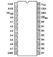
Pinout

  Connection Diagram


Specifications

DC Supply Voltage, VCC
(Voltages Referenced to Ground) . . . . . . . . . . . . . . . .      -0.5V to 7V
DC Input Diode Current, IIK
For VI < -0.5V or VI > VCC + 0.5V . . . . . . . . . . . . . . . . . . . . . .±20mA
DC Drain Current, IO
For -0.5V < VO < VCC + 0.5V. . . . . . . . . . . . . . . . . . . . . . . . . .±35mA
DC Output Diode Current, IOK
For VO < -0.5V or VO > VCC + 0.5V . . . . . . . . . . . . . . . . . . . . ±20mA
DC Output Source or Sink Current per Output Pin, IO
For VO > -0.5V or VO < VCC + 0.5V . . . . . . . . . . . . . . . . . . . . ±25mA
DC VCC or Ground Current, ICC . . . . . . . . . . . . . . . . . . . . . . . ±50mA


Description

The Harris CD74HC652 and CD74HCT652 three-state, octalbus transceiver/registers use silicon-gate CMOS technology to achieve operating speeds similar to LSTTL with the low power consumption of standard CMOS integrated circuits.

The CD74HC652 and CD74HCT652 have non-inverting outputs. CD74HCT652 consists of bus transceiver circuits, Dtype flip-flops, and control circuitry arranged for multiplexed transmission of data directly from the data bus or from the internal storage registers. Output Enables OEAB and OEBA are provided to control the transceiver functions. SAB and SBA control pins are provided to select whether real-time or stored data is transferred. The circuitry used for select control will eliminate the typical decoding glitch that occurs in a multiplexer during the transition between stored and real-time data. CD74HCT652 LOW input level selects real-time data, and a HIGH selects stored data. The following examples demonstrates the four fundamentals bus-management functions that can be performed with the octal-bus transceivers and registers.

Data on the A or B data bus, or both, can be stored in the internal D flip-flops by low-to-high transitions at the appropriate clock pins (CAB or CBA) regardless of the select of the control pins. When SAB and SBA are in the real-time transfer mode, it is also possible to store data without using the D-type flip-flops by simultaneously enabling OEAB and OEBA. In this configuration, each output reinforces CD74HCT652's input. Thus, when all other data sources to the two sets of bus lines are at high impedance, each set of bus lines will remain at its last state.


Customers Who Bought This Item Also Bought

Margin,quality,low-cost products with low minimum orders. Secure your online payments with SeekIC Buyer Protection.
Resistors
Fans, Thermal Management
Crystals and Oscillators
Prototyping Products
DE1
Batteries, Chargers, Holders
View more