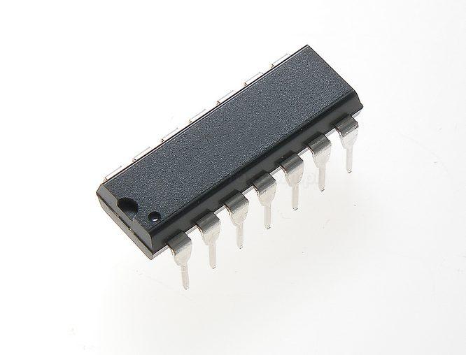
Features: `4.5-V to 5.5-V VCC Operation`Input Latches for BCD Code Storage`Blanking Capability`Phase Input for Complementing Outputs`Fanout (Over Temperature Range) Standard Outputs 10 LSTTL Loads`Balanced Propagation Delay and Transition Times`Significant Power Reduction, Compared to LSTTL Logi...
CD74HCT4543: Features: `4.5-V to 5.5-V VCC Operation`Input Latches for BCD Code Storage`Blanking Capability`Phase Input for Complementing Outputs`Fanout (Over Temperature Range) Standard Outputs 10 LSTTL Loads...
SeekIC Buyer Protection PLUS - newly updated for 2013!
268 Transactions
All payment methods are secure and covered by SeekIC Buyer Protection PLUS.
Supply voltage range, VCC . . . . . . . . . . . . . . . . . . . . . . . . . . . . . . . . . . . . . . . .0.5 V to 7 V
Input diode current, IIK (VI < 0.5 V or VI > VCC + 0.5 V) ) (see Note 1) . . . . . . . . ±20 mA
Output diode current, IOK (VO < 0.5 V or VO > VCC + 0.5V) (see Note 1) . . . . . . . ±20 mA
Continuous output source or sink current per output, IO (VO = 0 to VCC) . . . . . . . . .±25 mA
Continuous current through VCC or GND . . . . . . . . . . . . . . . . . . . . . . . . . . . . . . . . . .±50 mA
Package thermal impedance, JA (see Note 2) . . . . . . . . . . . . . . . . . . . . . . . . . . . . . 67°C/W
At distance 1/16 ± 1/32 in. (1.59 ± 0.79 mm) from case for 10 s maximum . . . . . . . . 265°C
Unit inserted into a PC board (min. thickness 1/16 in., 1.59 mm)
with solder contacting lead tips only . . . . . . . . . . . . . . . . . . . . . . . . . . . . . . . . . . . . . . 300°C
Storage temperature, Tstg . . . . . . . . . . . . . . . . . . . . . . . . . . . . . . . . . . . . . . . 65 to 150°C
† Stresses beyond those listed under "absolute maximum ratings" may cause permanent damage to the device. These are stress ratings only, and functional operation of the device at these or any other conditions beyond those indicated under "recommended operating conditions" is not implied. Exposure to absolute-maximum-rated conditions for extended periods may affect device reliability.
NOTES: 1. The input and output voltage ratings may be exceeded if the input and output current ratings are observed.
2. The package thermal impedance is calculated in accordance with JESD 51-7.
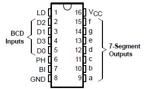
The CD74HCT4543 high-speed silicon-gate is a BCD-to-7 segment latch/decoder/driver designed primarily for directly driving liquid-crystal displays. While the latch enable (LD) is low, the latches are enabled to store the BCD inputs. When the latch enable is high, the latches are disabled, making the outputs transparent to the BCD inputs. CD74HCT4543 has an active-high blanking input (BI) and a phase input (PH) to which a square wave is applied for liquid-crystal applications. CD74HCT4543 square wave also is applied to the backplane of the liquid-crystal display.