CD74HCT40105

Features: • Independent Asynchronous Inputs and Outputs• Expandable in Either Direction• Reset Capability• Status Indicators on Inputs and Outputs• Three-State Outputs• Shift-Out Independent of Three-State Control• Fanout (Over Temperature Range) - Standar...

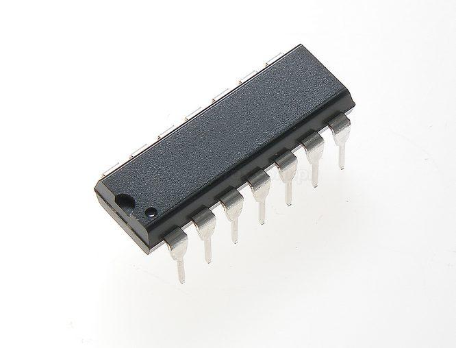
product image

CD74HCT40105 Picture
SeekIC No. : 004312153 Detail

CD74HCT40105: Features: • Independent Asynchronous Inputs and Outputs• Expandable in Either Direction• Reset Capability• Status Indicators on Inputs and Outputs• Three-State Outputs&...

floor Price/Ceiling Price

Part Number:
CD74HCT40105
Supply Ability:
5000

Price Break

  • Qty
  • 1~5000
  • Unit Price
  • Negotiable
  • Processing time
  • 15 Days
Total Cost: $ 0.00

SeekIC Buyer Protection PLUS - newly updated for 2013!

  • Escrow Protection.
  • Guaranteed refunds.
  • Secure payments.
  • Learn more >>

Month Sales

268 Transactions

Rating

evaluate  (4.8 stars)

Upload time: 2024/11/21

Payment Methods

All payment methods are secure and covered by SeekIC Buyer Protection PLUS.

Notice: When you place an order, your payment is made to SeekIC and not to your seller. SeekIC only pays the seller after confirming you have received your order. We will also never share your payment details with your seller.
Product Details

Description


Features:

• Independent Asynchronous Inputs and Outputs
• Expandable in Either Direction
• Reset Capability
• Status Indicators on Inputs and Outputs
• Three-State Outputs
• Shift-Out Independent of Three-State Control
• Fanout (Over Temperature Range)
   - Standard Outputs . . . . . . . . . . . . . . . 10 LSTTL Loads
   - Bus Driver Outputs . . . . . . . . . . . . . 15 LSTTL Loads
• Wide Operating Temperature Range . . . -55oC to 125oC
• Balanced Propagation Delay and Transition Times
• Significant Power Reduction Compared to LSTTL Logic ICs
• HC Types
   - 2V to 6V Operation
   - High Noise Immunity: NIL = 30%, NIH = 30% of VCC at VCC = 5V
• HCT Types
   - 4.5V to 5.5V Operation
   - Direct LSTTL Input Logic Compatibility,
    VIL= 0.8V (Max), VIH = 2V (Min)
   - CMOS Input Compatibility, Il 1A at VOL, VOH


Application

• Bit-Rate Smoothing
• CPU/Terminal Buffering
• Data Communications
• Peripheral Buffering
• Line Printer Input Buffers
• Auto-Dialers
• CRT Buffer Memories
• Radar Data Acquisition


Pinout

  Connection Diagram


Specifications

DC Supply Voltage, VCC . . . . . . . . . . . . . . . . . . . . . . . . -0.5V to 7V
DC Input Diode Current, IIK
For VI < -0.5V or VI > VCC + 0.5V . . . . . . . . . . . . . . . . . . . .±20mA
DC Output Diode Current, IOK
For VO < -0.5V or VO > VCC + 0.5V . . . . . . . . . . . . . . . . . . .±20mA
DC Output Source or Sink Current per Output Pin, IO
For VO > -0.5V or VO < VCC + 0.5V . . . . . . . . . . . . . . . . . . .±25mA
DC VCC or Ground Current, ICC . . . . . . . . . . . . . . . . . . . . . ±50mA


Description

The 'HC40105 and 'HCT40105 are high-speed silicon-gate CMOS devices that are compatible, except for "shift-out" circuitry, with the CD40105B. They are low-power first-in-out (FIFO) "elastic" storage registers that can store 16 four-bit words. The 40105 is capable of handling input and output data at different shifting rates. This feature makes CD74HCT40105 particularly useful as a buffer between asynchronous systems.

Each work position in the register is clocked by a control flipflop, which stores a marker bit. A "1" signifies that the position's data is filled and a "0" denotes a vacancy in that position. CD74HCT40105 control flip-flop detects the state of the preceding flip-flop and communicates its own status to the succeeding flip-flop. When a control flip-flop is in the "0" state and sees a "1" in the preceeding flip-flop, CD74HCT40105 generates a clock pulse that transfers data from the preceding four data latches into its own four data latches and resets the preceding flip-flop to "0". The first and last control flip-flops have buffered outputs.Since all empty locations "bubble" automatically to the input end, and all valid data ripple through to the output end, the status of the first control flip-flop (DATA-IN READY) indicates if the FIFO is full, and the status of the last flip-flop (DATAOUT READY) indicates if the FIFO contains data. As the earliest data are removed from the bottom of the data stack (the output end), all data entered later will automatically propagate (ripple) toward the output


Customers Who Bought This Item Also Bought

Margin,quality,low-cost products with low minimum orders. Secure your online payments with SeekIC Buyer Protection.
Line Protection, Backups
Connectors, Interconnects
Power Supplies - Board Mount
Cables, Wires
Cable Assemblies
View more