Features: * Edge-Triggered Data Flip-Flops
- Transparent Select Latches
* Buffered Inputs
* 3-State Complementary Outputs
* Bus Line Driving Capability
* Typical Propagation Delay: V = 5V, C = 15pF,CC LoT = 25 CA
- Clock to Output = 22ns
* Fanout (Over Temperature Range)
- Standard Outputs. . . . . . . . . . . . . . . 10 LSTTL Loads
- Bus Driver Outputs . . . . . . . . . . . . . 15 LSTTL Loadso o
* Wide Operating Temperature Range . . . -55 C to 125 C
* Balanced Propagation Delay and Transition Times
* Significant Power Reduction Compared to LSTTL Logic ICs
* 4.5V to 5.5V Operation
* Direct LSTTL Input Logic Compatibility,V = 0.8V (Max), V = 2V (Min) IL IH
* CMOS Input Compatibility, I 1 A at V , Vl OL OHPinout Specifications
DC Supply Voltage, VCC . . . . . . . . . . . . . . . . . . . . . . . . -0.5V to 7V
DC Input Diode Current, IIK
For V I < -0.5V or VI > V CC + 0.5V . . . . . . . . . . . . . . . . . ±20mA
DC Output Diode Current, I OK
For V O< -0.5V or V > V +0.5V . . . . . . . . . . . . . . . . . . . . . . . . 20mA
DC Drain Current, per Output, I O
For -0.5V < V O < V CC + 0.5V . . . . . . . . . . . . . . . . . . . . . . . . ±35mA
DC Output Source or Sink Current per Output Pin, IO
For VO > -0.5V or VO < V CC + 0.5V . . . . . . . . . . . . . . . . . . ±25mA
DC VCC or Ground Current, I CC . . . . . . . . . . . . . . . . . . . . . . . .±50mA
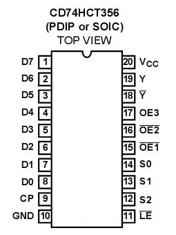
DescriptionThe CD74HCT356 consists of data selectors/multiplexers that select one of eight sources. The data select bits (S0, S1, and S2)arestoredintransparentlatchesthatareenabledbyalow latch enable input (LE).
CD74HCT356 data is stored in edge-triggered flip-flops that are triggered by a low-to-high clock transition.
In both types the 3-state outputs are controlled by three output-enable inputs (OE1, OE2, and OE3).

 CD74HCT356 Data Sheet


