Maximum Operating Temperature
: + 125 C
Mounting Style
: SMD/SMT
High Level Output Current
: - 4 mA
Low Level Output Current
: 4 mA
Supply Voltage - Max
: 5.5 V
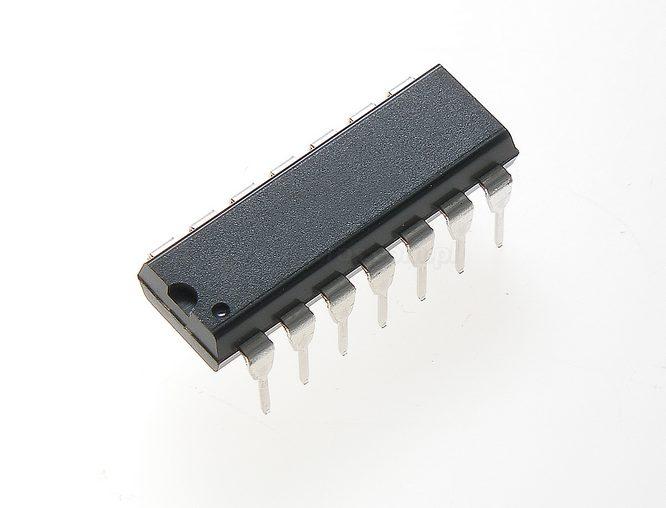
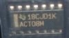
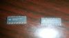
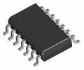
Package / Case
: SOIC-14
Product
: NOR
Supply Voltage - Min
: 4.5 V
Packaging
: Tube
Number of Lines (Input / Output)
: 3 / 1
Logic Family
: 74HCT
Number of Gates
: Triple
Propagation Delay Time
: 23 ns
DescriptionThe CD74HCT27M logic gates utilize silicon gate CMOS technology to achieve operating speeds similar to LSTTL gates with the low power consumption of standard CMOS integrated circuits. The features of CD74HCT27M can be summarized as (1)Buffered Inputs; (2)Typical Propagation Delay: 7ns at VCC = 5V, CL = 15pF, TA = 25oC; (3)Fanout (Over Temperature Range): Standard Outputs: 10 LSTTL Loads, Bus Driver Outputs: 15 LSTTL Loads; (4)Wide Operating Temperature Range . . . -55oC to 125oC; (5)Balanced Propagation Delay and Transition Times; (6)Significant Power Reduction Compared to LSTTL Logic ICs; (7)HC Types: 2V to 6V Operation, High Noise Immunity: NIL = 30%, NIH = 30% of VCC at VCC = 5V; (8)HCT Types: 4.5V to 5.5V Operation, Direct LSTTL Input Logic Compatibility, VIL= 0.8V (Max), VIH = 2V (Min); (9)CMOS Input Compatibility, Il1A at VOL, VOH.
The absolute maximum ratings of the CD74HCT27M are: (1)DC supply voltage, VCC: -0.5V to 7V; (2)DC input diode current, IIK for VI < -0.5V or VI > VCC + 0.5V: ±20mA; (3)DC output diode current, IOK for VO < -0.5V or VO > VCC + 0.5V: ±20mA; (4)DC output source or sink current per output Pin, IO For VO > -0.5V or VO < VCC + 0.5V: ±25mA; (5)DC VCC or ground current, ICC or IGND: ±50mA.
The following is about the electrical characteristics of CD74HCT27M: (1)High Level Input Voltage: 1.5V min; (2)low Level Input Voltage: 0.5V max; (3)High Level Output Voltage CMOS Loads: 1.9V min at VIH or VIL, IO= -0.02mA; (4)High Level Output Voltage TTL Loads: 3.98V min at VIH or VIL, IO= -4mA; (5)Low Level Output Voltage CMOS Loads: 0.1V max at VIH or VIL, IO=0.02mA; (6)Low Level Output Voltage TTL Loads: 0.26V max at VIH or VIL, IO=0.02mA; (7)Input Leakage Current: ±0.1A max at VCC or GND; (8)Quiescent Device Current: 8A max at VCC or GND.
 CD74HCT27M Data Sheet