Product
: AND
Number of Gates
: 4
Maximum Operating Temperature
: + 125 C
Number of Lines (Input / Output)
: 2 / 1
High Level Output Current
: - 4 mA
Low Level Output Current
: 4 mA
Supply Voltage - Max
: 5.5 V
Supply Voltage - Min
: 4.5 V
Packaging
: Tube
Mounting Style
: Through Hole
Package / Case
: PDIP-14
Logic Family
: 74HCT
Propagation Delay Time
: 25 ns
DescriptionThe CD74HCT139M96 contains two independent binary to one of four decoders each with a single active low enable input (1E or 2E). Data on the select inputs (1A0 and 1A1 or 2A0 and 2A1) cause one of the four normally high outputs to go low. The features of CD74HCT139M96 are as follows: (1)Buffered Inputs and Outputs; (2)Typical Propagation Delay: 13ns (Data to Output at VCC = 5V, CL = 15pF, TA = 25oC; (3)Serial or Parallel Expansion Without External Gating; (4)Fanout (Over Temperature Range): Standard Outputs:10 LSTTL Loads, Bus Driver Outputs: 15 LSTTL Loads; (5)Wide Operating Temperature Range: -55oC to 125oC; (6)Balanced Propagation Delay and Transition Times; (7)Significant Power Reduction Compared to LSTTL Logic ICs; (8)HC Types: 2V to 6V Operation, High Noise Immunity: NIL = 30%, NIH = 30%of VCC at VCC = 5V; (9)HCT Types: 4.5V to 5.5V Operation, Direct LSTTL Input Logic Compatibility, VIL= 0.8V (Max), VIH = 2V (Min); (10)CMOS Input Compatibility, Il 1A at VOL, VOH.
The absolute maximum ratings of the CD74HCT139M96 are: (1)DC supply voltage, VCC: -0.5V to 7V; (2)DC input diode current, IIK for VI < -0.5V or VI > VCC + 0.5V: ±20mA; (3)DC output diode current, IOK for VO < -0.5V or VO > VCC + 0.5V: ±20mA; (4)DC output source or sink current per output Pin, IO For VO > -0.5V or VO < VCC + 0.5V: ±25mA; (5)DC VCC or ground current, ICC or IGND: ±50mA.
The following is about the electrical characteristics of CD74HCT139M96: (1)High Level Input Voltage: 1.5V min; (2)low Level Input Voltage: 0.5V max; (3)High Level Output Voltage CMOS Loads: 1.9V min at VIH or VIL, IO= -0.02mA; (4)High Level Output Voltage TTL Loads: 3.98V min at VIH or VIL, IO= -4mA; (5)Low Level Output Voltage CMOS Loads: 0.1V max at VIH or VIL, IO=0.02mA; (6)Low Level Output Voltage TTL Loads: 0.26V max at VIH or VIL, IO=0.02mA; (7)Input Leakage Current: ±0.1A max at VCC or GND; (8)Quiescent Device Current: 8A max at VCC or GND.
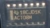
Parameters: | Technical/Catalog Information | CD74HCT08E |
| Vendor | Texas Instruments |
| Category | Integrated Circuits (ICs) |
| Number of Circuits | 4 - Quad |
| Package / Case | 14-DIP (300 mil) |
| Logic Type | AND Gate |
| Packaging | Tube |
| Mounting Type | Through Hole |
| Number of Inputs | 2 |
| Current - Output High, Low | 5.2mA, 5.2mA |
| Supply Voltage | 4.5 V ~ 5.5 V |
| Operating Temperature | -55°C ~ 125°C |
| Voltage - Supply | 4.5 V ~ 5.5 V |
| Drawing Number | 296; 4040049; N; 14, 16, 18, 20 |
| Lead Free Status | Lead Free |
| RoHS Status | RoHS Compliant |
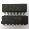
| Other Names | CD74HCT08E
CD74HCT08E
296 2084 5 ND
29620845ND
296-2084-5
|
 CD74HCT08E Data Sheet