CD74HC4051-EP

Features: Controlled Baseline One Assembly/Test Site, One Fabrication SiteExtended Temperature Performance of55°C to 125°CEnhanced Diminishing Manufacturing Sources (DMS) SupportEnhanced Product Change NotificationQualification Pedigree†Wide Analog Input Voltage Range of ±5 V MaxLow ON Resis...

product image

CD74HC4051-EP Picture
SeekIC No. : 004312040 Detail

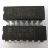
CD74HC4051-EP: Features: Controlled Baseline One Assembly/Test Site, One Fabrication SiteExtended Temperature Performance of55°C to 125°CEnhanced Diminishing Manufacturing Sources (DMS) SupportEnhanced Product Cha...
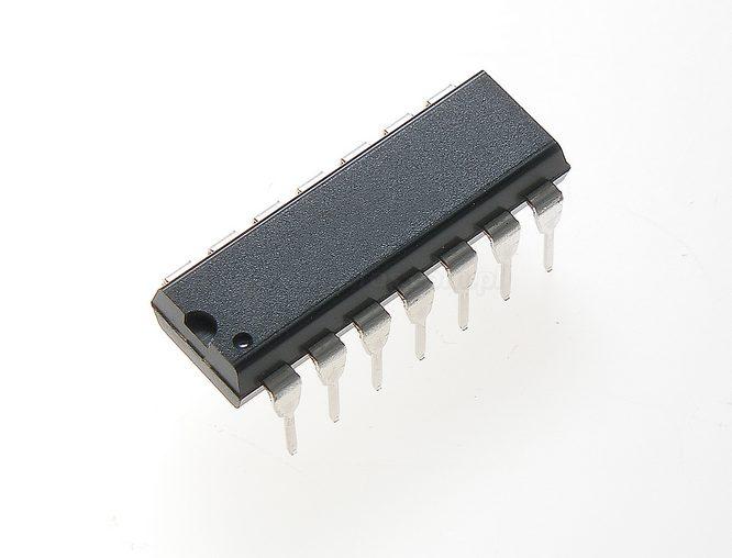
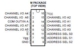
floor Price/Ceiling Price

Part Number:
CD74HC4051-EP
Supply Ability:
5000

Price Break

  • Qty
  • 1~5000
  • Unit Price
  • Negotiable
  • Processing time
  • 15 Days
Total Cost: $ 0.00

SeekIC Buyer Protection PLUS - newly updated for 2013!

  • Escrow Protection.
  • Guaranteed refunds.
  • Secure payments.
  • Learn more >>

Month Sales

268 Transactions

Rating

evaluate  (4.8 stars)

Upload time: 2024/10/17

Payment Methods

All payment methods are secure and covered by SeekIC Buyer Protection PLUS.

Notice: When you place an order, your payment is made to SeekIC and not to your seller. SeekIC only pays the seller after confirming you have received your order. We will also never share your payment details with your seller.
Product Details

Description


Features:

Controlled Baseline
One Assembly/Test Site, One Fabrication Site
Extended Temperature Performance of
55°C to 125°C
Enhanced Diminishing Manufacturing Sources (DMS) Support
Enhanced Product Change Notification
Qualification Pedigree†
Wide Analog Input Voltage Range of ±5 V Max
Low ON Resistance
70 Typical (VCC VEE = 4.5 V)
40 Typical (VCC VEE = 9 V)
Low Crosstalk Between Switches
Fast Switching and Propagation Speeds
Break-Before-Make Switching
Operation Control Voltage = 2 V to 6 V
Switch Voltage = 0 V to 10 V
High Noise Immunity NIL = 30%, NIH = 30% of VCC, VCC = 5 V


Pinout

  Connection Diagram


Specifications

Supply voltage range, VCC VEE (see Note 1) . . . . . . . . . . . . . . . . . . . . . . . . . . . . . . . . . . 0.5 V to 10.5 V
Supply voltage range, VCC . . . . . . . . . . . . . . . . . . . . . . . . . . . . . . . . . . . . . . . . . . . . . . . . . . . . 0.5 V to 7 V
Supply voltage range, VEE . . . . . . . . . . . . . . . . . . . . . . . . . . . . . . . . . . . . . . . . . . .. . . . . . . . +0.5 V to 7 V
Input clamp current, IIK (VI < 0.5 V or VI > VCC + 0.5 V) . . . . . . . . . . . . . . . . . . . . . . . . . . . . . . . . ±20 mA
Output clamp current, IOK (VO < VEE 0.5 V or VO > VCC + 0.5 V) . . . . . . . . . . . . . . . . . . . . . . . . . . ±20 mA
Switch current (VI > VEE 0.5 V or VI < VCC + 0.5 V) . . . . . . . . . . . . . . . . . . . . . . . . . . . . . . . . . . . . ±25 mA
Continuous current through VCC or GND . . . . . . . . . . . . . . . . . . . . . . . . . . . . . . .  . . . . . . . . . . . . . . ±50 mA
VEE current, IEE . . . . . . . . . . . . . . . . . . . . . . . . . . . . . . . . . . . . . . . . . . . . . . . . . . . . . . . . . . . . . . . . . 20 mA
Package thermal impedance, JA (see Note 2): M package . . . . . . . . . . . . . . . . . . . . . .  . . . . . . . . . 73°C/W
Maximum junction temperature, TJ . . . . . . . . . . . . . . . . . . . . . . . . . . . . . . . . . . . . .. . . . . . . . . . . . . . . 150°C
Lead temperature (during soldering):
At distance 1/16 ± 1/32 inch (1,59 ± 0,79 mm) from case for 10 s max . . . . . . . . . . . . . . . . . . . . . . . 300°C
Storage temperature range, Tstg . . . . . . . . . . . . . . . . . . . . . . . . . . . . . . . . . . . . . . . . . . . . 65°C to 150°C
† Stresses beyond those listed under "absolute maximum ratings" may cause permanent damage to the device. These are stress ratings only, and functional operation of the device at these or any other conditions beyond those indicated under "recommended operating conditions" is not implied. Exposure to absolute-maximum-rated conditions for extended periods may affect device reliability.
NOTES: 1. All voltages referenced to GND unless otherwise specified.
2. The package thermal impedance is calculated in accordance with JESD 51-7.


Description

CD74HC4051-EP is a digitally controlled analog switch that utilizes silicon gate CMOS technology to achieve operating speeds similar to LSTTL, with the low power consumption of standard CMOS integrated circuits.

This CD74HC4051-EP analog multiplexer/demultiplexer controls analog voltages that may vary across the voltage supply range (i.e., VCC to VEE). These bidirectional switches allow any analog input to be used as an output and vice versa. The switches have low ON resistance and low OFF leakages. In addition, the device has an enable control (E) that, when high, disables all switches to their OFF state.


Customers Who Bought This Item Also Bought

Margin,quality,low-cost products with low minimum orders. Secure your online payments with SeekIC Buyer Protection.
Cables, Wires
Resistors
Batteries, Chargers, Holders
Boxes, Enclosures, Racks
Sensors, Transducers
View more