Features: • Maximum Frequency, Typically 60MHz
CL = 15pF, VCC = 5V, TA = 25oC
• Positive-Edge Clocking
• Overriding Reset
• Buffered Inputs and Outputs
• Fanout (Over Temperature Range)
- Standard Outputs . . . . . . . . . . . . . . . . .10 LSTTL Loads
- Bus Driver Outputs . . . . . . . . . . . . . . . .15 LSTTL Loads
• Wide Operating Temperature Range . . . -55oC to 125oC
• Balanced Propagation Delay and Transition Times
• Significant Power Reduction Compared to LSTTL
Logic ICs
• HC Types
- 2V to 6V Operation
- High Noise Immunity: NIL = 30%, NIH = 30% of VCC
at VCC = 5VApplicationAudio
Automotive
Broadband
Digital Control
Military
Optical Networking
Security
Telephony
Video & Imaging
WirelessPinout Specifications
DC Supply Voltage, VCC . . . . . . . . . . . . . . . . . . . . . . . . . . . .-0.5V to 7V
DC Input Diode Current, IIK
For VI< -0.5V or VI> VCC+ 0.5V. . . . . . . . . . . . . . . . . . . . . . . . .±20mA
DC Output Diode Current, IOK
For VO< -0.5V or VO> VCC+ 0.5V. . . . . . . . . . . . . . . . . . . . . . . . .±20mA
DC Output Source or Sink Current per Output Pin, IO
For VO > -0.5V or VO < VCC + 0.5V . . . . . . . . . . . . . . . . . . . . . . . ±25mA
DC VCC or Ground Current, ICC . . . . . . . . . . . . . . . . . . . . . . . . . . ±50mA
DescriptionThe 'HC4015 consists of two identical, independent, 4-stage serial-input/parallel-output registers. Each register has independent Clock (CP) and Reset (MR) inputs as well as a single serial Data input. "Q" outputs are available from each of the four stages on both registers. All register stages are Dtype, master-slave flip-flops. The logic level present at the Data input is transferred into the first register stage and shifted over one stage at each positive- going clock transition. Resetting of all stages is accomplished by a high level on the reset line.
The CD74HC4015 can drive up to 10 low power Schottky equivalent loads. The 'HC4015 is an enhanced version of equivalent CMOS types.The 'HC4015 consists of two identical, independent, 4-stage serial-input/parallel-output registers. Each register has independent Clock (CP) and Reset (MR) inputs as well as a single serial Data input. "Q" outputs are available from each of the four stages on both registers. All CD74HC4015 register stages are Dtype, master-slave flip-flops. The logic level present at the Data input is transferred into the first register stage and shifted over one stage at each positive- going clock
transition. Resetting of all stages is accomplished by a high level on the reset line.
The CD74HC4015 can drive up to 10 low power Schottky equivalent loads. The 'HC4015 is an enhanced version of equivalent CMOS types.

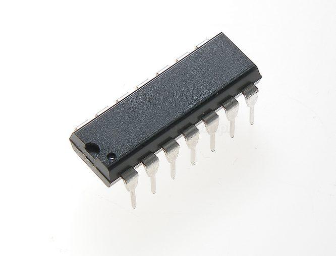
 CD74HC4015 Data Sheet