Features: • Digital Design Avoids Analog Compensation Errors
• Easily Cascadable for Higher Order Loops
• Useful Frequency Range
- K-Clock . . . . . . . . . . . . . . . . . . . . . . . . . . DC to 55MHz (Typ)
- I/D-Clock . . . . . . . . . . . . . . . . . . . . . . . DC to 35MHz (Typ)
• Dynamically Variable Bandwidth
• Very Narrow Bandwidth Attainable
• Power-On Reset
• Output Capability
- Standard. . . . . . . . . . . . . . . . . . . . . . XORPDOUT, ECPDOUT
- Bus Driver . . . . . . . . . . . . . . . . . . . . . . . .. . . . . . . . I/DOUT
• Fanout (Over Temperature Range)
- Standard Outputs . . . . . . . . . . . . . . . . . . . . 10 LSTTL Loads
- Bus Driver Outputs . . . . . . . . . . . . . . . . .. 15 LSTTL Loads
• Balanced Propagation Delay and Transition Times
• Significant Power Reduction Compared to LSTTL
Logic ICs
• 'HC297 Types
- Operation Voltage . . . . . . . . . . . . . . . . . . . . . . . . . . . 2 to 6V
- High Noise Immunity NIL = 30%, NIH = 30% of VCC at 5V
• CD74HCT297 Types
- Operation Voltage . . . . . . . . . . . . . . . . . . . . . . . . 4.5 to 5.5V
- Direct LSTTL Input Logic Compatibility
VIL = 0.8V (Max), VIH = 2V (Min)
- CMOS Input Compatibility II 1A at VOL, VOHApplicationAudio
Automotive
Broadband
Digital Control
Military
Optical Networking
Security
Telephony
Video & Imaging
WirelessPinout Specifications
DC Supply Voltage, VCC. . . . . . . . . . . . . . . . . . . . .-0.5V to 7V
DC Input Diode Current, IIK
For VI<-0.5V or VI> VCC+0.5V. . . . . . . . . . . . . . . . . . .±20mA
DC Output Diode Current, IOK
For VO<-0.5V or VO>VCC+0.5V . . . . . . . . . . . . . . . . . . .±20mA
DC Drain Current, per Output, IO
For -0.5V < VO < VCC + 0.5V. . . . . . . . . . . . . . . . . . .±25MA
DC Output Source or Sink Current per Output Pin, IO
For VO>-0.5V or VO< VCC+ 0.5V. . . . . . . . . . . . . . . . . . ±25mA
DC VCC or Ground Current, ICC . . . . . . . . . . . . . . . . . . . ±50mA
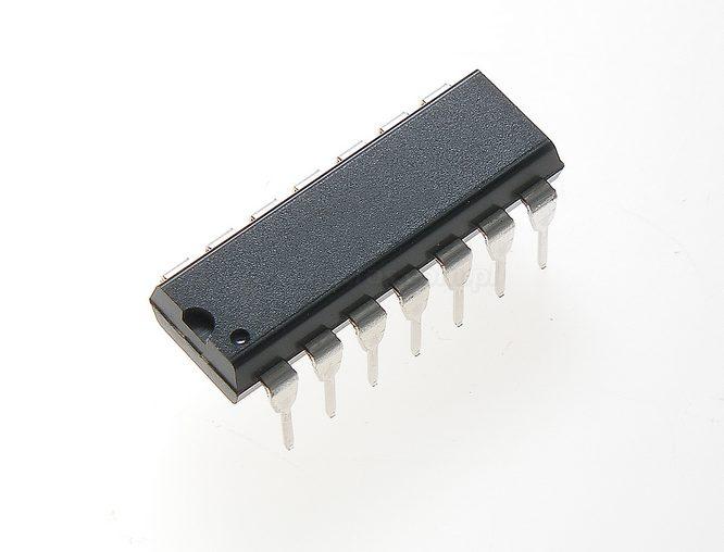
DescriptionThe 'HC297 and CD74HCT297 are high-speed silicon gate CMOS devices that are pin-compatible with low power Schottky TTL (LSTTL).
These CD74HC297 are designed to provide a simple, cost-effective solution to high-accuracy, digital, phase-locked-loop applications. They contain all the necessary circuits, with the exception of the divide-by-N counter, to build first-order phase-locked-loops.
Both EXCLUSIVE-OR (XORPD) and edge-controlled phase detectors (ECPD) are provided for maximum flexibility. The CD74HC297 input signals for the EXCLUSIVE-OR phase detector must have a 50% duty factor to obtain the maximum lock-range.
Proper partitioning of the loop function, with many of the building blocks external to the package, makes it easy for the designer to incorporate ripple cancellation (see Figure 2) or to cascade to higher order phase-locked-loops.
CD74HC297 length of the up/down K-counter is digitally programmable according to the K-counter function table. With A, B, C and D all LOW, the K-counter is disabled. With A HIGH and B, C and D LOW, the K-counter is only three stages long, which widens the bandwidth or capture range and shortens the lock time of the loop. When A, B, C and D are all programmed HIGH, the K-counter becomes seventeen stages long, which narrows the bandwidth or capture range and lengthens the lock time. CD74HC297 Real-time control of loop bandwidth by manipulating the A to D inputs can maximize the overall performance of the digital phase-locked-loop.
The 'HC297 and CD74HCT297 can perform the classic first order phase-locked-loop function without using analog components. The accuracy of the digital phase-locked-loop (DPLL) is not affected by VCC and temperature variations but depends solely on accuracies of the K-clock and loop propagation delays.

 CD74HC297 Data Sheet


