Maximum Operating Temperature
: + 125 C
Polarity
: Non-Inverting
Input Type
: Single-Ended
Output Type
: Single-Ended
Mounting Style
: Through Hole
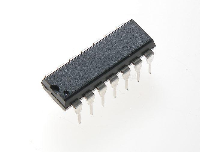
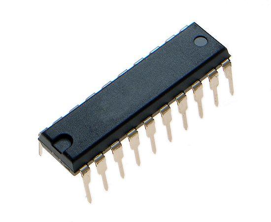
Package / Case
: PDIP-20
Packaging
: Tube
Number of Circuits
: 8
Logic Type
: D-Type Flip-Flop
Logic Family
: 74HC
Supply Voltage - Max
: 6 V
High Level Output Current
: - 5.2 mA
Low Level Output Current
: 5.2 mA
Propagation Delay Time
: 150 ns
DescriptionThe CD74HC273E high speed octal D-Type flip-flops with a direct clear input are manufactured with silicon-gate CMOS technology. The features of CD74HC273E are as follows: (1)Common Clock and Asynchronous Master Reset; (2)Positive Edge Triggering; (3)Buffered Inputs; (4)Fanout (Over Temperature Range): Standard Outputs: 10 LSTTL Loads, Bus Driver Outputs: 15 LSTTL Loads; (5)CD74HC273E Wide Operating Temperature Range: -55oC to 125oC; (6)Balanced Propagation Delay and Transition Times; (7)Significant Power Reduction Compared to LSTTL Logic ICs; (8)HC Types: 2V to 6V Operation, High Noise Immunity: NIL = 30%, NIH = 30% of VCC at VCC = 5V; (9)HCT Types: 4.5V to 5.5V Operation, Direct LSTTL Input Logic Compatibility, VIL= 0.8V (Max), VIH = 2V (Min), CMOS Input Compatibility, Il1A at VOL, VOH.
The absolute maximum ratings of the CD74HC273E are: (1)DC supply voltage, VCC: -0.5V to 7V; (2)DC input diode current, IIK for VI < -0.5V or VI > VCC + 0.5V: ±20mA; (3)DC output diode current, IOK for VO < -0.5V or VO > VCC + 0.5V: ±20mA; (4)DC output source or sink current per output Pin, IO For VO > -0.5V or VO < VCC + 0.5V: ±25mA; (5)DC VCC or ground current, ICC or IGND: ±50mA.
The following is about the electrical characteristics of CD74HC273E: (1)High Level Input Voltage: 1.5V min; (2)low Level Input Voltage: 0.5V max; (3)High Level Output Voltage CMOS Loads: 1.9V min at VIH or VIL, IO= -0.02mA; (4)High Level Output Voltage TTL Loads: 3.98V min at VIH or VIL, IO= -4mA; (5)Low Level Output Voltage CMOS Loads: 0.1V max at VIH or VIL, IO=0.02mA; (6)Low Level Output Voltage TTL Loads: 0.26V max at VIH or VIL, IO=0.02mA; (7)Input Leakage Current: ±0.1A max at VCC or GND; (8)Quiescent Device Current: 8A max at VCC or GND.
 CD74HC273E Data Sheet