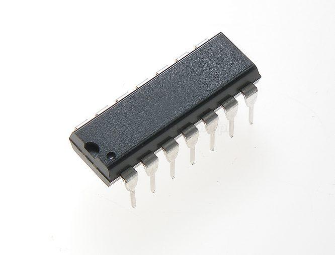
Features: • CD54/74FCT373, CD54/74FCT373AT - Non-Inverting• CD54/74FCT533 - Inverting• Buffered inputs• Typical Propagation Delay: 3.9ns at VCC = 5V, TA = +25oC, CL = 50pF (FCT373AT)• SCR-Latchup-Resistant BiCMOS Process and Circuit Design• FCTXXX Types - Speed ...
CD74FCT533: Features: • CD54/74FCT373, CD54/74FCT373AT - Non-Inverting• CD54/74FCT533 - Inverting• Buffered inputs• Typical Propagation Delay: 3.9ns at VCC = 5V, TA = +25oC, CL = 50pF (F...
SeekIC Buyer Protection PLUS - newly updated for 2013!
268 Transactions
All payment methods are secure and covered by SeekIC Buyer Protection PLUS.
The CD54/74FCT373, 373AT, and 533 octal transparent latches use a small-geometry BiCMOS technology. The output stage is a combination of bipolar and CMOS transistors that limits the output-HIGH level to two diode drops below VCC. This resultant lowering of output swing (0V to 3.7V) reduces power bus ringing (a source of EMI) and minimizes VCC bounce and ground bounce and their effects during simultaneous output switching. The output configuration also enhances switching speed and is capable of sinking 32mA to 48mA.
The CD54/74FCT373, 373AT, and 533 outputs are transparent to the inputs when the Latch Enable (LE) is HIGH. When the Latch Enable (LE) goes LOW, the data is latched. The Output Enable (OE) controls the three-state outputs. When the Output Enable (OE) is HIGH, the outputs are in the highimpedance state. The latch operation is independent of the state of the Output Enable.