CD54HC365

Features: Buffered InputsHigh Current Bus Driver OutputsTypicalPropagationDelaytPLH ,tPHL =8nsatVCC=5V, CL = 15pF, TA = 25Fanout (Over Temperature Range) - Standard Outputs. . . . . . . . . . . . . . . 10 LSTTL Loads - Bus Driver Outputs . . . . . . . . . . . . . 15 LSTTL LoadsWide Operating Tempe...

product image

CD54HC365 Picture
SeekIC No. : 004311674 Detail

CD54HC365: Features: Buffered InputsHigh Current Bus Driver OutputsTypicalPropagationDelaytPLH ,tPHL =8nsatVCC=5V, CL = 15pF, TA = 25Fanout (Over Temperature Range) - Standard Outputs. . . . . . . . . . . . . ...

floor Price/Ceiling Price

Part Number:
CD54HC365
Supply Ability:
5000

Price Break

  • Qty
  • 1~5000
  • Unit Price
  • Negotiable
  • Processing time
  • 15 Days
Total Cost: $ 0.00

SeekIC Buyer Protection PLUS - newly updated for 2013!

  • Escrow Protection.
  • Guaranteed refunds.
  • Secure payments.
  • Learn more >>

Month Sales

268 Transactions

Rating

evaluate  (4.8 stars)

Upload time: 2024/12/25

Payment Methods

All payment methods are secure and covered by SeekIC Buyer Protection PLUS.

Notice: When you place an order, your payment is made to SeekIC and not to your seller. SeekIC only pays the seller after confirming you have received your order. We will also never share your payment details with your seller.
Product Details

Description


Features:

Buffered Inputs
High Current Bus Driver Outputs
TypicalPropagationDelaytPLH ,tPHL =8nsatVCC=5V,
  CL  = 15pF, TA  = 25
Fanout (Over Temperature Range)
   - Standard Outputs. . . . . . . . . . . . . . . 10 LSTTL Loads
   - Bus Driver Outputs . . . . . . . . . . . . . 15 LSTTL Loads
 Wide Operating Temperature Range . . . -55 to 125
Balanced Propagation Delay and Transition Times
Significant Power Reduction Compared to LSTTLLogic ICs
HC Types
   - 2V to 6V Operation
   - High Noise Immunity: NIL = 30%, NIH = 30% of VCCat VCC= 5V
HCT Types
   - 4.5V to 5.5V Operation
   - Direct LSTTL Input Logic Compatibility,
   VIL = 0.8V (Max), VIH= 2V (Min)
   - CMOS Input Compatibility, Il1Aat VOL ,VOH


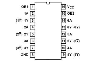
Pinout

  Connection Diagram


Specifications

DC Supply Voltage, VCC. . . . . . . . . . . . . . . . . . . . . -0.5V to 7V
DC Input Diode Current, IIK
     For VI< -0.5V or V> VCC + 0.5V . . . . . .  . . . . . . . .±20mA
DC Output Diode Current, IOK
     For VO< -0.5V or VO> VCC + 0.5V . . . . . . . . . . . . . .±20mA
DC Drain Current, per Output, IO
     For -0.5V < VO < VCC + 0.5V . . . . . . . . .  . . . . . . . .±35mA
DC Output Source or Sink Current per Output Pin, IO
     For VO > -0.5V or VO< VCC + 0.5V . . . . . . . . . . .  . .±25mA
DC VCC or Ground Current, ICC   . . . . .. . . . . . . . . . . . .±50mA


Description

The 'HC365, 'HCT365, and 'HC366 silicon gate CMOS three-state buffers are general purpose high-speed non-invertingand inverting buffers. They have high drive current outputswhich enable high speed operation even when driving largebus capacitances. These circuits possess the low powerdissipation of CMOS circuitry, yet have speedscomparable tolow power Schottky TTL circuits. Both circuits are capable ofdriving up to 15 low power Schottky inputs.

The 'HC365 and 'HCT365 are non-inverting buffers, whereasthe 'HC366 is an inverting buffer. These devices have twothree-state control inputs (OE1 and OE2) which are NORedtogether to control all six gates.

The 'HCT365 logic families are speed, function and pincompatible with the standard LS logic family.


Customers Who Bought This Item Also Bought

Margin,quality,low-cost products with low minimum orders. Secure your online payments with SeekIC Buyer Protection.
Batteries, Chargers, Holders
Audio Products
Programmers, Development Systems
Cable Assemblies
Computers, Office - Components, Accessories
View more