Features: Wide supply voltage range: 3.0V to 15V
High noise immunity: 0.45 VDD (typ.)
Low power TTL fan out of 2 driving 74L
compatibility or 1 driving 74LS
Serial to parallel capability
Storage register capability
Random (addressable) data entry
Active high demultiplexing capability
Common active high clearPinout SpecificationsIf Military/Aerospace specified devices are required,
please contact the National Semiconductor Sales
Office/Distributors for availability and specifications.
DC Supply Voltage (VDD).............. b0.5V to a18 VDC
Input Voltage (VIN) ............. .b0.5V to VDD a0.5 VDC
Storage Temperature (TS).................... 65to 150
Power Dissipation (PD)
Dual-In-Line .....................................700 mW
Small Outline .....................................500 mW
Lead Temperature (TL)
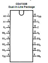
(Soldering, 10 seconds) ...................................260 DescriptionThe CD4723B is a dual 4-bit addressable latch with com-mon control inputs, including two address inputs (A0, A1),an active low enable input (E ), and an active high clear input(CL). CD4723B Each latch has a data input (D) and four outputs (Q0Q3). The CD4724B is an 8-bit addressable latch with threeaddress inputs (A0A2), an active low enable input (E), ac- tive high clear input (CL), a data input (D) and eight outputs(Q0Q7).
Data is entered into a particular bit in the latch when that isaddressed by the address inputs and the enable E islow.CD4723B Data entry is inhibited when enable Eishigh.
When clear (CL) and enable E are high, all outputs are low.When clear (CL) is high and enable Eis low. thechanneldemultiplexing occurs. The bit that is addressed has an ac-tive output which follows the data input while all unad-dressed bits are held low. When operating in the address-able latch mode (E e CL e low), changing morthan onebit of the address could impose a transient wrong address.Therefore, CD4723B should only be done whileinthememorymode (E e high, CL e low).

 CD4723BM Data Sheet


