CD4517B

DescriptionThe CD4517B dual 64-stage static shift register consists of two independent registers each having a clock, data, and write enable input and outputs accessible at taps following the 16th,32th, and 64th stages.These taps also serve as input points allowing data to be inputted at the 17th,...

product image

CD4517B Picture
SeekIC No. : 004311413 Detail

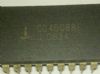
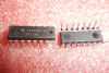
CD4517B: DescriptionThe CD4517B dual 64-stage static shift register consists of two independent registers each having a clock, data, and write enable input and outputs accessible at taps following the 16th,3...

floor Price/Ceiling Price

Part Number:
CD4517B
Supply Ability:
5000

Price Break

  • Qty
  • 1~5000
  • Unit Price
  • Negotiable
  • Processing time
  • 15 Days
Total Cost: $ 0.00

SeekIC Buyer Protection PLUS - newly updated for 2013!

  • Escrow Protection.
  • Guaranteed refunds.
  • Secure payments.
  • Learn more >>

Month Sales

268 Transactions

Rating

evaluate  (4.8 stars)

Upload time: 2024/6/10

Payment Methods

All payment methods are secure and covered by SeekIC Buyer Protection PLUS.

Notice: When you place an order, your payment is made to SeekIC and not to your seller. SeekIC only pays the seller after confirming you have received your order. We will also never share your payment details with your seller.
Product Details

Description


Description

The CD4517B dual 64-stage static shift register consists of two independent registers each having a clock, data, and write enable input and outputs accessible at taps following the 16th,32th, and 64th stages.These taps also serve as input points allowing data to be inputted at the 17th, 33rd, and 49th stages when the write enable inputs is a logic 1 and the clock goes through a low-to-high transition.

Features of the CD4517B are:(1)low quiescent current; (2)100% tested for quiescent current at 20 V; (3)clock frequency 12 MHz typ at Vdd is 10 V; (4)maximum input current of 1 uA at 18 V over full package-temperature range;100 nA at 18 V and 25; (5)standardized, symmetrical output characteristics; (6)Schmitt trigger clock inputs allow operation with very slow clock clock rise and fall times; (7)three-state outputs.

The absolute maximum ratings of the CD4517B can be summarized as:(1): DC supply-voltage range(VDD) is -0.5 V to +20 V(voltages referenced to Vss terminal); (2): input voltage range, all inputs is -0.5 V to VDD+0.5 V; (3): DC input current, any one input is ±10 mA; (4): operating temperature range(Ta) is -55 to +125; (5): storage temperature range(Tstg) is -65 to +150.


Customers Who Bought This Item Also Bought

Margin,quality,low-cost products with low minimum orders. Secure your online payments with SeekIC Buyer Protection.
Inductors, Coils, Chokes
Motors, Solenoids, Driver Boards/Modules
Semiconductor Modules
Optical Inspection Equipment
Transformers
Fans, Thermal Management
View more