CD4508BMS

Features: • High-Voltage Types (20-Volt Rating)• Two Independent 4-Bit Latches• Individual Master Reset for Each 4-Bit Latch• 3-State Outputs with High-Impedance State for Bus Line Applications• Medium-Speed Operation: tPHL = tPLH = 70nS (Typ.) at VDD = 10V and CL = 5...

product image

CD4508BMS Picture
SeekIC No. : 004311397 Detail

CD4508BMS: Features: • High-Voltage Types (20-Volt Rating)• Two Independent 4-Bit Latches• Individual Master Reset for Each 4-Bit Latch• 3-State Outputs with High-Impedance State for Bu...

floor Price/Ceiling Price

Part Number:
CD4508BMS
Supply Ability:
5000

Price Break

  • Qty
  • 1~5000
  • Unit Price
  • Negotiable
  • Processing time
  • 15 Days
Total Cost: $ 0.00

SeekIC Buyer Protection PLUS - newly updated for 2013!

  • Escrow Protection.
  • Guaranteed refunds.
  • Secure payments.
  • Learn more >>

Month Sales

268 Transactions

Rating

evaluate  (4.8 stars)

Upload time: 2024/5/28

Payment Methods

All payment methods are secure and covered by SeekIC Buyer Protection PLUS.

Notice: When you place an order, your payment is made to SeekIC and not to your seller. SeekIC only pays the seller after confirming you have received your order. We will also never share your payment details with your seller.
Product Details

Description


Features:

• High-Voltage Types (20-Volt Rating)
• Two Independent 4-Bit Latches
• Individual Master Reset for Each 4-Bit Latch
• 3-State Outputs with High-Impedance State for Bus Line Applications
• Medium-Speed Operation: tPHL = tPLH = 70nS (Typ.) at VDD = 10V and CL = 50pF
• 100% Tested for Quiescent Current at 20V
• 5V, 10V, and 15V Parametric Ratings
• Standardized, Symmetrical Output Characteristics
• Maximum Input Current of 1A at 18V Over Full Package Temperature Range; 100nA at 18V and 25oC
• Noise Margin (Full Package-Temperature Range):
- 1V at VDD = 5V
- 2V at VDD = 10V
- 2.5V at VDD = 15V
• Meets all Requirements of JEDEC Tentative Standard No. 13B, "Standard Specifications for Description of 'B' Series
   CMOS Devices"


Application

• Buffer Storage
• Holding Registers
• Data Storage and Multiplexing


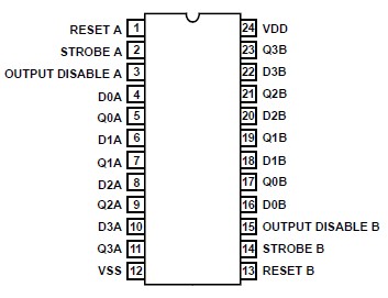
Pinout

  Connection Diagram


Specifications

DC Supply Voltage Range, (VDD) . . . . . . . . . . . . .   . .  . .  . . . .  -0.5V to +20V
(Voltage Referenced to VSS Terminals)
Input Voltage Range, All Inputs . . . . . . . . . . . . .  . .  .. .  . .-0.5V to VDD +0.5V
DC Input Current, Any One Input . . . . . . . . . . . . . .  . .   . .  . . . . . . . . .±10mA
Operating Temperature Range. . . . . . . . . . . . .  . .  . .  . .  . .  -55oC to +125oC
Package Types D, F, K, H
Storage Temperature Range (TSTG) . . . . . . . . . . . .  . .  . .  . .-65oC to +150oC
Lead Temperature (During Soldering) . . . . . . . . . . . . . . . .  . .  . .  . . . . +265oC
At Distance 1/16 ± 1/32 Inch (1.59mm ± 0.79mm) from case for 10s Maximum


Description

CD4508BMS dual 4-bit latch contains two identical 4-bit latches with separate STROBE, RESET, and OUTPUT DISABLE controls. With the STROBE line in the high state, the data on the "D" inputs appear at the corresponding "Q" outputs provided the DISABLE line is in the low state. Changing the STROBE line to the low state locks the data into the latch. A high on the reset line forces the outputs to a low level regardless of the state of the STROBE input. The outputs are forced to the high-impedance state for bus line applications by a high level on the DISABLE input.

The CD4508BMS is supplied in these 24 lead outline packages: Braze Seal DIP H4V Frit Seal DIP H1Z Ceramic Flatpack H4P


Customers Who Bought This Item Also Bought

Margin,quality,low-cost products with low minimum orders. Secure your online payments with SeekIC Buyer Protection.
RF and RFID
Resistors
Inductors, Coils, Chokes
Potentiometers, Variable Resistors
Undefined Category
Batteries, Chargers, Holders
View more