CD4504BMS

Features: * High Voltage Type (20V Rating)* Independence of Power Supply Sequence Consider-ations- VCC can Exceed VDD- Input Signals can Exceed Both VCC and VDD* Up and Down Level Shifting Capability* Shiftable Input Threshold for Either CMOS or TTLCompatibility* 100% Tested for Quiescent Current ...

product image

CD4504BMS Picture
SeekIC No. : 004311394 Detail

CD4504BMS: Features: * High Voltage Type (20V Rating)* Independence of Power Supply Sequence Consider-ations- VCC can Exceed VDD- Input Signals can Exceed Both VCC and VDD* Up and Down Level Shifting Capabilit...

floor Price/Ceiling Price

Part Number:
CD4504BMS
Supply Ability:
5000

Price Break

  • Qty
  • 1~5000
  • Unit Price
  • Negotiable
  • Processing time
  • 15 Days
Total Cost: $ 0.00

SeekIC Buyer Protection PLUS - newly updated for 2013!

  • Escrow Protection.
  • Guaranteed refunds.
  • Secure payments.
  • Learn more >>

Month Sales

268 Transactions

Rating

evaluate  (4.8 stars)

Upload time: 2024/6/10

Payment Methods

All payment methods are secure and covered by SeekIC Buyer Protection PLUS.

Notice: When you place an order, your payment is made to SeekIC and not to your seller. SeekIC only pays the seller after confirming you have received your order. We will also never share your payment details with your seller.
Product Details

Description


Features:

* High Voltage Type (20V Rating)
* Independence of Power Supply Sequence Consider-
ations
- VCC can Exceed VDD
- Input Signals can Exceed Both VCC and VDD
* Up and Down Level Shifting Capability
* Shiftable Input Threshold for Either CMOS or TTL
Compatibility
* 100% Tested for Quiescent Current at 20V
* 5V, 10V and 15V Parametric Ratings
* Standardized Symmetrical Output Characteristics
* Maximum Input Current of 1A at 18V Over Full Pack-
o
age Temperature Range; 100nA at 18V and +25 C
* Meets All Requirements of JEDEC Tentative Standard
No. 13B, "Standard Specifications for Description of
'B' Series CMOS Devices"


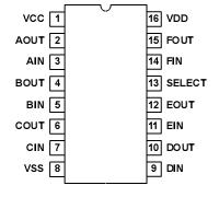
Pinout

  Connection Diagram


Specifications

DC Supply Voltage Range, (VDD) . . . . . . . . . . . . . . . -0.5V to +20V
(Voltage Referenced to VSS Terminals)
Input Voltage Range, All Inputs . . . . . . . . . . . . .-0.5V to VDD +0.5V
DC Input Current, Any One Input . . . . . . . . . . . . . . . . . .. ..±10mA
Operating Temperature Range. . . . . . . . . . . . . . . . -55 to +125
Package Types D, F, K, H
Storage Temperature Range (TSTG). . . . . . . . . . . -65 to +150
Lead Temperature (During Soldering) . . . . . . . . . . . . . . . . . +265


Description

CD4504BMS hex voltage level shifter consists of six circuits which shift input signals from the VCC logic level to the VDD logic level. To shift TTL signals to CMOS logic levels, the SELECT input is at the VCC HIGH logic state. When the SELECT input is at a LOW logic state, each circuit translates signals from one CMOS level to another. The CD4504BMS is supplied in these 16-lead outline packages: Frit Seal DIP H1F Ceramic Flatpack H6W


Customers Who Bought This Item Also Bought

Margin,quality,low-cost products with low minimum orders. Secure your online payments with SeekIC Buyer Protection.
Cables, Wires
Semiconductor Modules
Industrial Controls, Meters
Audio Products
Computers, Office - Components, Accessories
Cables, Wires - Management
View more