Features: • High Voltage Type (20V Rating)
• Retriggerable/Resettable Capability
• Trigger and Reset Propagation Delays Independent of RX, CX
• Triggering from Leading or Trailing Edge
• Q and Q Buffered Outputs Available
• Separate Resets
• Wide Range of Output Pulse Widths
• 100% Tested for Quiescent Current at 20V
• 5V, 10V and 15V Parametric Ratings
• Standardized Symmetrical Output Characteristics
• Maximum Input Current of 1A at 18V Over Full Package Temperature Range; 100nA at 18V and +25oC
• Noise Margin (Over Full Package/Temperature Range)
1V at VDD = 5V
2V at VDD = 10V
2.5V at VDD = 15V
• Meets All Requirements of JEDEC Tentative Standard No. 13B, "Standard Specifications for Description of 'B' Series CMOS Devices"
Application• Pulse Delay and Timing
• Pulse Shaping
Pinout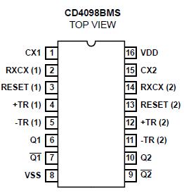 SpecificationsDC Supply Voltage Range, (VDD)..0.5V to +20V (Voltage Referenced to VSS Terminals)
Input Voltage Range, All Inputs .....................................................-0.5V to VDD +0.5V
DC Input Current, Any One Input.......................................................................±10mA
Operating Temperature Range ................. -55 to +125 Package Types D, F, K, H
Storage Temperature Range (TSTG).................................................. -65 to +150
Lead Temperature (During Soldering) ............................................................. +265
At Distance 1/16 ± 1/32 Inch (1.59mm ± 0.79mm) from case for 10s MaximumDescriptionCD4098BMS dual monostable multivibrator provides stable retriggerable/resettable one shot operation for any fixed voltage timing application. CD4098BMS external resistor (RX) and an external capacitor (CX) control the timing for the circuit. Adjustment of RX and CX provides a wide range of output pulse widths from the Q and Q terminals. The time delay from trigger input to output transition (trigger propagation delay) and the time delay from reset input to output transition (reset propagation delay) are independent of RX and CX. Leading edge triggering (+TR) and trailing edge triggering (-TR) inputs are provided for triggering from either edge of an input pulse. An unused +TR input should be tied to VSS. An unused -TR input should be tied to VDD. A RESET (on low level) is provided for immediate termination of the output pulse or to prevent output pulses when power is turn unused RESET input should be tied to VDD. However, if an entire section of the CD4098BMS is not used, CD4098BMS's RESET should be tied to VSS. See Table 9. In normal operation the circuit triggers (extends the output pulse one period) on the application of each new trigger pulse. For operation in the non-retriggerable mode, Q is connected to -TR when leading edge triggering (+TR) is used or Q is connected to +TR when trailing edge triggering (-TR) is used. The time period (T) for this multivibrator can be approximated by: TX = 1/2RXCX for CX 3 0.01F. Time periods as a function of RX for values of CX and VDD are given in Figure 8. Values of T vary from unit to unit and as a function of voltage, temperature, and RXCX. The CD4098BMS minimum value of external resistance, RX, is 5k. The CD4098BMS maximum value of external capacitance, CX, is 100F. Figure 9 shows time periods as a function of CX for values of RX and VDD. The CD4098BMS output pulse width has variations of ±2.5% typically, over the temperature range of -55oC to +125oC for CX = 1000pF and RX = 100k. For power supply variations of ±5%, the output pulse width has variations of ±0.5% typically, for VDD = 10V and 15V and &pulsmn;1% typically, for VDD = 5V at CX = 1000pF and RX = 5k. The CD4098BMS is supplied in these 16-lead outline packages: Braze Seal DIP H4T Frit Seal DIP H1F Ceramic Flatpack H6W

 CD4098BMS Data Sheet