Number of Gates
: 4
Maximum Operating Temperature
: + 125 C
Number of Lines (Input / Output)
: 2 / 1
Product
: NAND
Packaging
: Tube
Mounting Style
: Through Hole
Package / Case
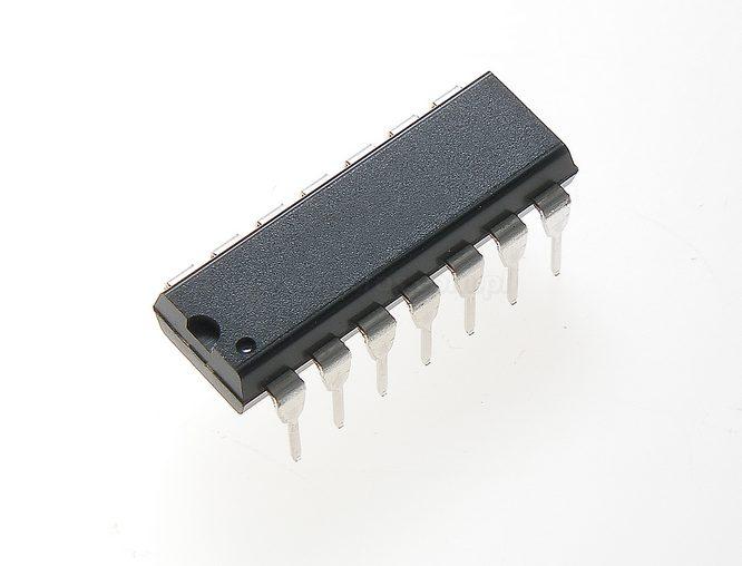
: PDIP-14
High Level Output Current
: - 4.2 mA
Low Level Output Current
: 4.2 mA
Supply Voltage - Max
: 18 V
Supply Voltage - Min
: 3 V
Logic Family
: CD4000
Propagation Delay Time
: 380 ns
Pinout Description
The CD4093BE belongs to CD4093B family which consists of four Schrnitt- trigger circuits. Each circuit functions as a two-input NAND gate with Schmitt-trigger action on both inputs. The CD4093BE gate switches at different points for positive- and negative-going signals. The difference between the positive voltage (Vp) and the negative voltage (VN) is defined as hysteresis voltage (VH) (see Fig. 2). The CD4093B types are supplied in 14-lead hermetic dual-in-line ceramic packages (F3A suffix), 14-lead dual-in-line plastic packages (E suffix), 14-lead small-outline packages MT M96, and NSR suffixes), and 14-lead thin shrink small-outline packages (PW and PWR suffixes).
The features of CD4093BE can be summarized as (1)schmitt-trigger action on each input with no external components; (2)hysteresis voltage typically 0.9 at VDD=5V and VDD=10V; (3)noise immunity ter than 50%; (4)no limit on input rise and fall times; (5)standardized, syrnmetri output characteristics; (6)100% tested for quiescent current at 20V; (7)CD4093BE maximum input current of 1A at 18V over full package-temperature range, 100 nA at 18V and 25°C; (8)5-V, 10-V, and 15-V parametric ratings; (9)meets all requirements of JEDEC; (10)standard No. 13B. "standard specifications for description of 'B' series CMOS devices".
The absolute maximum ratings of CD4093BE are (1)DC supply-voltage range, (VDD) voltages referenced To VSS terminal): -0.5V to +20V; (2)input voltage range, all inputs: -0.5V to VDD +0.5V; (3)DC input current, anyone input: ±10mA; (4)package thermal impedance, JA(see note 1)E package: 80°C/W,; (5)M package: 86°C/W, NS package 76°C/W; (6)device dissipation per output transistor for Ta=full package-temperature range (all package types): 100mW; (7)CD4093BE operattng-jemperature range (Ta): -55°C to +125°C; (8)storage temperature range (Tstg): -65°C to +150°C; (9)lead temperature (during sqldering): At distance 1/1 6±1/32 inch (1.59 =±0.79rnm) from case for 10s max: +265°C.(NOTE 1: Package thermal impedance is calculated in accordance with JESD 51-7).
The CD4093BE types are supplied in 14-lead hermetic dual-in-line ceramic packages (F3A suffix), 14-lead dual-in-line plastic packages (E suffix), 14-lead small-outline packages (M, MT, M96, and NSR suffixes), and 14-lead thin shrink small-outline packages (PW and PWR suffixes).
Features of the CD4093BE are:(1)schmitt-trigger action on each input with no external components;(2)hysteresis voltage typically 0.9 V at VDD=5V and 1.3V at VDD=10V;(3)noise immunity greater than 50%;(4)no limit on input rise and fall times;(5)standardized,symmeterical output characteristics;(6)100% tested for quiescent current at 20V;(7)maximum input current of 1A at 18V over full package-temperature range;(8)5V,10V and 15V parametric ratings;(9)meets all requirements of JEDEC.
The absolute maximum ratings of the CD4093BE can be summarized as:(1):the symbol is VDD,the parameter is supply voltage range,the value is -0.5 to +20,the unit is V;(2):the symbol is VI,the parameter is input voltage range,the value is -0.5 to VDD+0.5,the unit is V;(3):the symbol is IIN,the parameter is DC input current,the value is ±10,the unit is mA;(4):the symbol is TA,the parameter is operating temperature range,the value is -55 to +125,the unit is ;(5):the symbol is Tstg,the parameter is storage temperature range,the value is -65 to +150,the unit is ;(6):the symbol is TL,the parameter is lead temperature for soldering purposes,1/16±1/32 inch from case for 10 seconds,the value is +265,the unit is .
Parameters: | Technical/Catalog Information | CD4093BE |
| Vendor | Texas Instruments |
| Category | Integrated Circuits (ICs) |
| Number of Circuits | 4 - Quad |
| Package / Case | 14-DIP (300 mil) |
| Logic Type | NAND Gate - Schmitt Trigger |
| Packaging | Tube |
| Mounting Type | Through Hole |
| Number of Inputs | 2 |
| Current - Output High, Low | 6.8mA, 6.8mA |
| Supply Voltage | 3 V ~ 18 V |
| Operating Temperature | -55°C ~ 125°C |
| Voltage - Supply | 3 V ~ 18 V |
| Drawing Number | 296; 4040049; N; 14, 16, 18, 20 |
| Lead Free Status | Lead Free |
| RoHS Status | RoHS Compliant |
| Other Names | CD4093BE
CD4093BE
296 2068 5 ND
29620685ND
296-2068-5
|
 CD4093BE Data Sheet