Switch Configuration
: SPST
Maximum Operating Temperature
: + 125 C
Mounting Style
: SMD/SMT
Number of Switches
: 4
Switch Voltage (Max)
: 15 V
Package / Case
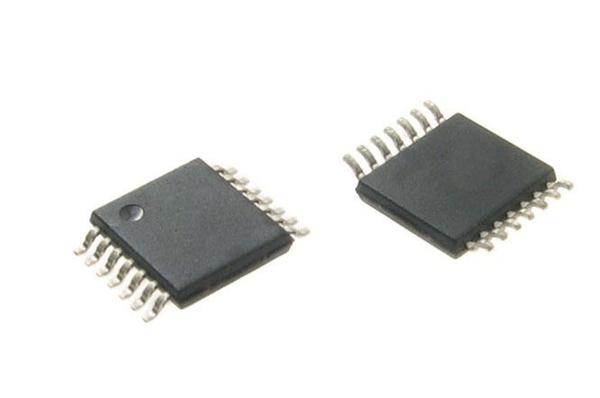
: TSSOP-14
On Time (Max)
: 70 ns
On Resistance (Max)
: 1050 Ohms
Off Time (Max)
: 70 ns
Operating Supply Voltage
: 3 V to 18 V
Pinout Description
The CD4066BPWG4 consists of two identical, independent data-type flip-flops.Each flip-flop has independent data, set,reset, and clock inputs and Q and Q outputs.CD4066BPWG4 can be used for shift register applications abd by connecting Q output to the data input, for counter and toggle applications. The features of the CD4066BPWG4 are: (1)15-V Digital or ±7.5-V Peak-to-PeakSwitching ; (2)125- Typical On-State Resistance for 15-VOperation ; (3)Switch On-State Resistance Matched toWithin 5 Over 15-V Signal-Input Range ; (4)On-State Resistance Flat Over FullPeak-to-Peak Signal Range ; (5)High On/Off Output-Voltage Ratio: 80 dBTypical at fis = 10 kHz, RL = 1 k; (6)High Degree of Linearity: <0.5% DistortionTypical at fis= 1 kHz, Vis= 5 Vp-p,VDD VSS 10 V, RL = 10 k.
The following is about the absolute maximum ratings of CD4066BPWG4: (1)DC supply-voltage range, VDD: -0.5V to 20V; (2)input voltage range, Vis: -0.5V to VDD+0.5V; (3)DC input current, IIN: ±10mA; (4)CD4066BPWG4 package thermal impredance, JA: E package 80/W, M package 86/W, NS package 76/W, PW package 113/W; (5)CD4066BPWG4 lead temperature: 265; (6)storage temperature range: -65 to 150.
The electrical characteristics of the CD4066BPWG4 are: (1)VILC control input, low voltage(max): 1V max at VDD=5V; (2)VIHC control input, low voltage: 3.5(min)V max at VDD=5V; (3)CD4066BPWG4 input current(max): ±0.1Amax at VisVDD, VDD-VSS=18V, VCCVDD-VSS, VDD=18V; (4)crosstalk: 50mV min at VDD=10V; (5)turn-on and turn-off propagation delay: 35ns typical and 70ns max; (6)CD4066BPWG4 maximum control input repetition rate: 6MHz min at VDD=5V.
Parameters: | Technical/Catalog Information | CD4066BPWG4 |
| Vendor | Texas Instruments |
| Category | Integrated Circuits (ICs) |
| Circuit | 1 x 1:1 |
| Independent Circuits | 4 |
| Mounting Type | Surface Mount |
| Current - Output High, Low | - |
| Package / Case | 14-TSSOP |
| Packaging | Tube |
| Type | Bilateral, FET Switches |
| Voltage Supply Source | Dual Supply |
| Operating Temperature | -55°C ~ 125°C |
| Voltage - Supply | 3 V ~ 18 V |
| Drawing Number | 296; 4040064; PW; 8, 14, 16, 20, 24, 28 |
| Lead Free Status | Lead Free |
| RoHS Status | RoHS Compliant |
| Other Names | CD4066BPWG4
CD4066BPWG4
|

 CD4066BPWG4 Data Sheet


