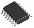
Maximum Operating Temperature
: + 125 C
Mounting Style
: SMD/SMT
Packaging
: Reel
Number of Circuits
: 2
Input Type
: Single-Ended
Logic Type
: D-Type Flip-Flop
Polarity
: Inverting/Non-Inverting
Output Type
: Differential
Package / Case
: SOIC-14
Logic Family
: CD4000
Propagation Delay Time
: 300 ns
High Level Output Current
: - 4.2 mA
Low Level Output Current
: 4.2 mA
Supply Voltage - Max
: 18 V
Pinout
 Description
The CD4013BM96 is designed as one kind of CMOS dual 'D'-type flip-flops which consists of two identical independent data-type flip-flops. Each flip-flop has independent data, set, reset, and clock inputs and Q and /Q outputs.
CD4013BM96 has nine features. (1)Set-reset capability. (2)Static flip-flop operation retains state indefinitely with clock level either "high" or "low". (3)Medium-speed operation 16MHz clock toggle rate at 10V. (4)Standardized symmetrical output characteristics. (5)100% tested for quiescent current at 20V. (6)Maximum input current of 1uA at 18V over full package temperature range; 100na at 18V and 25°C. (7)Noise margin (over full package temperature range): 1V at Vdd=5V and 2V at Vdd=10V and 2.5V at Vdd=15V. (8)5V, 10V and 15V parametric ratings. (9)Meets all requirements of JEDEC tentatice standard No.13B, "standard specifications for description of 'B' series CMOS devices". Those are all the main features.
Some absolute maximum ratings CD4013BM96 have been concluded into several points as follow. (1)Its DC supply voltage range would be from -0.5V to 20V. (2)Its input voltage range all inputs would be from -0.5V to Vdd+0.5V. (3)Its DC input current any one input would be +/-10mA. (4)Its power dissipation per package would be 500mW. (5)Its device dissipation per output transistor would be 100mW. (6)Its operating temperature range would be from -55°C to 125°C. (7)Its storage temperature range would be from -65°C to 150°C. (8)Its lead temperature during soldering would be 265°C. It should be noted that stresses above those listed in absolute maximum ratings may cause permanent damage to device.
Also some CD4013BM96 dynamic electrical characteristics at Vdd=5V are concluded as follow. (1)Its transition time would be typ 100ns and max 200ns. (2)Its maximum clock input frequency would be min 3.5MHz and typ 7MHz. (3)Its minimum clock pulse width would be typ 70ns and max 140ns. And so on. If you have any question or suggestion or want to know more information please contact us for details. Thank you!
Parameters: | Technical/Catalog Information | CD4013BM96 |
| Vendor | Texas Instruments (VA) |
| Category | Integrated Circuits (ICs) |
| Mounting Type | Surface Mount |
| Package / Case | 14-SOIC (3.9mm Width), 14-SOL |
| Function | Set and Reset |
| Number of Bits per Element | 1 |
| Number of Elements | 2 - Dual |
| Current - Output High, Low | 6.8mA, 6.8mA |
| Output Type | Differential |
| Trigger Type | Positive Edge |
| Type | D-Type |
| Packaging | Digi-Reel? |
| Operating Temperature | -55°C ~ 125°C |
| Delay Time - Propagation | 45ns |
| Frequency - Clock | 24MHz |
| Voltage - Supply | 3 V ~ 18 V |
| Drawing Number | * |
| Lead Free Status | Lead Free |
| RoHS Status | RoHS Compliant |
| Other Names | CD4013BM96
CD4013BM96
296 24347 6 ND
296243476ND
296-24347-6
|

 CD4013BM96 Data Sheet


