Number of Gates
: 4
Maximum Operating Temperature
: + 125 C
Number of Lines (Input / Output)
: 2 / 1
Product
: NAND
Packaging
: Tube
Mounting Style
: Through Hole
Package / Case
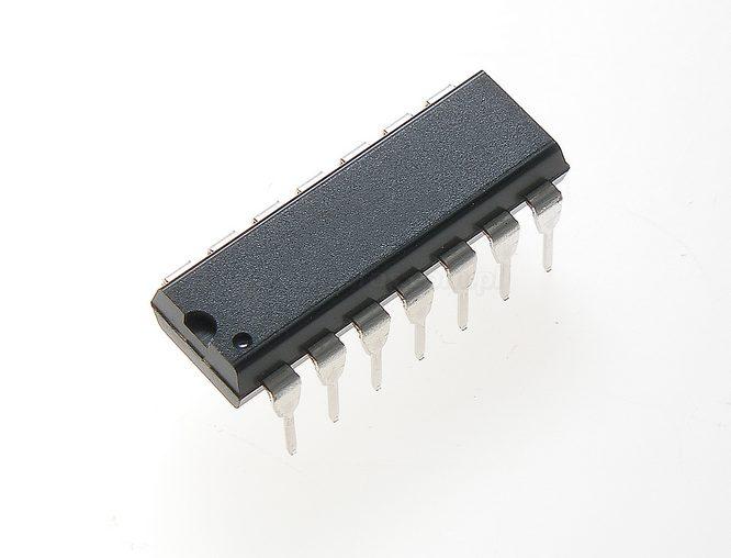
: PDIP-14
High Level Output Current
: - 4.2 mA
Low Level Output Current
: 4.2 mA
Propagation Delay Time
: 250 ns
Supply Voltage - Max
: 18 V
Supply Voltage - Min
: 3 V
Logic Family
: CD40
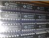
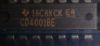
DescriptionThe CD4011BE belongs to CD4011B family. CD4011B, CD4012B, and CD4023B NAND gates provide the system designer with direct implementation of the NAND function and supplement the existing family of CMOS gates. All inputs and outputs are buffered. The CD4011B, CD4012B, and CD4023B types are supplied in 14-lead hermetic dual-in-line ceramic packages (F3A suffix), 14-lead dual-in-line plastic packages (E suffix), 14-lead small-outline packages MT, M96, and NSR suffixes), and 14-lead thin shrink small-outline packages (PWR suffix). The CD4011B and CD4023B types also are supplied in 14-lead thin shrink small-outline packages (PW suffix).
The features of CD4011BE can be summarized as (1)propagation delay time = 60 ns(typ.) at CL=50 pF, Vpp =10V; (2)buffered inputs and outputs; (3)standardized symmetrical output characteristics; (4)maximum input currant of 1 A at 18V over full package; temperature range; 100nA at 18V and 25°C; (5)100% tasted for quiaseant current at 20V; (6)5-V, 10-V, and 15-V parametric ratings; (7)noise margin lover full package temperature range: 1 V at VDD = 5V; 2V at VDD=10V; 2.5V at VDD=15V; (8)meetS all requirements of JEDEC Tentative standard No.13B, "Standard Specifications for Description of "B" Series CMOS Devices".
The absolute maximum ratings of CD4011BE are (1)DC supply-voltage range, (VDD) voltages referenced to VSS terminal: -0.5V to +20V; (2)input voltage range, all inputs: -0.5V to VDD +0.5V; (3)DC input current, any one input: ±10mA; (4)power dissipation per package(PD): for TA=-55°C to +100°C: 500mW, for TA=+100°C to +125°C: derate linearity at 12mW/°C to 200mW; (5)device dissipation per output transistor for TA=full package-temperature range (all package types): 100mW; (6)operating-temperature range (TA): -50°C to +125°C; (7)storage temperature range (Tstg): -65°C to + 150°C; (8)lead temperature (during soldering): at distance 1/16 ± 1/32 inch (1.59 ± 0.79mm) from case for 10s max: +265°C.
Parameters: | Technical/Catalog Information | CD4011BE |
| Vendor | Texas Instruments |
| Category | Integrated Circuits (ICs) |
| Number of Circuits | 4 - Quad |
| Package / Case | 14-DIP (300 mil) |
| Logic Type | NAND Gate |
| Packaging | Tube |
| Mounting Type | Through Hole |
| Number of Inputs | 2 |
| Current - Output High, Low | 6.8mA, 6.8mA |
| Supply Voltage | 3 V ~ 18 V |
| Operating Temperature | -55°C ~ 125°C |
| Voltage - Supply | 3 V ~ 18 V |
| Drawing Number | 296; 4040049; N; 14, 16, 18, 20 |
| Lead Free Status | Lead Free |
| RoHS Status | RoHS Compliant |
| Other Names | CD4011BE
CD4011BE
296 2031 5 ND
29620315ND
296-2031-5
|
 CD4011BE Data Sheet