CD4010C

Features: `Wide supply voltage range: ....3.0V to 15V`Low power:........... 100 nW (typ.)`High noise immunity: ......0.45 VDD (typ.)` High current sinking: .8 mA (min.) at VO = 0.5V capability: ............and VDD = 10VApplication• Automotive• Data terminals• Instrumentation̶...

product image

CD4010C Picture
SeekIC No. : 004311173 Detail

CD4010C: Features: `Wide supply voltage range: ....3.0V to 15V`Low power:........... 100 nW (typ.)`High noise immunity: ......0.45 VDD (typ.)` High current sinking: .8 mA (min.) at VO = 0.5V capability: .......

floor Price/Ceiling Price

Part Number:
CD4010C
Supply Ability:
5000

Price Break

  • Qty
  • 1~5000
  • Unit Price
  • Negotiable
  • Processing time
  • 15 Days
Total Cost: $ 0.00

SeekIC Buyer Protection PLUS - newly updated for 2013!

  • Escrow Protection.
  • Guaranteed refunds.
  • Secure payments.
  • Learn more >>

Month Sales

268 Transactions

Rating

evaluate  (4.8 stars)

Upload time: 2024/5/28

Payment Methods

All payment methods are secure and covered by SeekIC Buyer Protection PLUS.

Notice: When you place an order, your payment is made to SeekIC and not to your seller. SeekIC only pays the seller after confirming you have received your order. We will also never share your payment details with your seller.
Product Details

Description


Features:

`Wide supply voltage range: ....3.0V to 15V
`Low power:........... 100 nW (typ.)
`High noise immunity: ......0.45 VDD (typ.)
` High current sinking: .8 mA (min.) at VO = 0.5V
   capability: ............and VDD = 10V


Application

• Automotive
• Data terminals
• Instrumentation
• Medical electronics
• Alarm system
• Industrial controls
• Remote metering
• Computers


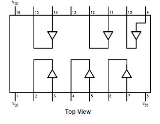
Pinout

  Connection Diagram


Specifications

Voltage at Any Pin (Note 2) .....VSS − 0.3V to VSS +15.5V
Operating Temperature Range .........−45 to +85
Storage Temperature Range (TS) .......−65 to +150
Power Dissipation (PD)
Dual-In-Line ................. .....700 mW
Small Outline ......................500 mW
Lead Temperature (TL)
(Soldering, 10 seconds) ..................260
Operating Range (VDD) ..........VSS + 3V to VSS + 15V

Note 1: "Absolute Maximum Ratings indicate limits beyond which damage to the device may occur. Operating Ratings indicate conditions for which the device is functional, but do not guarantee specific performance limits."

Note 2: This device should not be connected to circuits with the power on because high transient voltage may cause permanent damage.


Description

The CD4010C hex buffers are monolithic complementary MOS (CMOS) integrated circuits. The N- and P-channel enhancement mode transistors provide a symmetrical circuit with output swings essentially equal to the supply voltage. This results in high noise immunity over a wide supply voltage range. No DC power other than that caused by leakage current is consumed during static conditions. CD4010C All inputs are protected against static discharge. CD4010C gates may be used as hex buffers, CMOS to DTL or TTL interface or as CMOS current drivers. Conversion ranges are from 3V to 15V providing VCC VDD. The devices also have buffered outputs which improve transfer characteristics
by providing very high gain.


Customers Who Bought This Item Also Bought

Margin,quality,low-cost products with low minimum orders. Secure your online payments with SeekIC Buyer Protection.
Connectors, Interconnects
Memory Cards, Modules
Integrated Circuits (ICs)
Cables, Wires
View more