CD40104BMS

Features: • High Voltage Type (20V Rating)• Medium Speed fCL = 12MHz (typ.) at VDD = 10V• Fully Static Operation• Synchronous Parallel or Serial Operation• Three State Outputs (CD40104BMS)• Asynchronous Master Reset (CD40194BMS)• 5V, 10V and 15V Parametric...

product image

CD40104BMS Picture
SeekIC No. : 004311164 Detail

CD40104BMS: Features: • High Voltage Type (20V Rating)• Medium Speed fCL = 12MHz (typ.) at VDD = 10V• Fully Static Operation• Synchronous Parallel or Serial Operation• Three State ...

floor Price/Ceiling Price

Part Number:
CD40104BMS
Supply Ability:
5000

Price Break

  • Qty
  • 1~5000
  • Unit Price
  • Negotiable
  • Processing time
  • 15 Days
Total Cost: $ 0.00

SeekIC Buyer Protection PLUS - newly updated for 2013!

  • Escrow Protection.
  • Guaranteed refunds.
  • Secure payments.
  • Learn more >>

Month Sales

268 Transactions

Rating

evaluate  (4.8 stars)

Upload time: 2024/11/24

Payment Methods

All payment methods are secure and covered by SeekIC Buyer Protection PLUS.

Notice: When you place an order, your payment is made to SeekIC and not to your seller. SeekIC only pays the seller after confirming you have received your order. We will also never share your payment details with your seller.
Product Details

Description


Features:

• High Voltage Type (20V Rating)
• Medium Speed fCL = 12MHz (typ.) at VDD = 10V
• Fully Static Operation
• Synchronous Parallel or Serial Operation
• Three State Outputs (CD40104BMS)
• Asynchronous Master Reset (CD40194BMS)
• 5V, 10V and 15V Parametric Ratings
• Standardized Symmetrical Output Characteristics
• Meets All Requirements of JEDEC Tentative Standard No. 13B, "Standard Specifications for Description of 'B' Series CMOS Devices"


Application

• Arithmetic Unit Bus Registers
• Serial/Parallel Conversions
• General Purpose Register for Bus Organized Systems
• General Purpose Registers


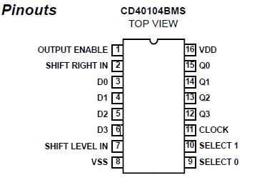
Pinout

  Connection Diagram


Specifications

DC Supply Voltage Range, (VDD) . . . . . . . . . . .. . . . .  . . . . .  . . . . -0.5V to +20V
(Voltage Referenced to VSS Terminals)
Input Voltage Range, All Inputs . . . . . . . . . . . . . . . . . . .. . . .-0.5V to VDD +0.5V
DC Input Current, Any One Input . . . . . . . .. . . . . .  . . . . . . . . . . . . . . . .±10mA
Operating Temperature Range. . . . . . . . . . . .. . . . . . . . . . . . . . -55 to +125
Package Types D, F, K, H
Storage Temperature Range (TSTG) . . . . . .. . . . . . . . . .  . . . . . -65 to +150
Lead Temperature (During Soldering) . . . . . . . . . . . . . . . . .. . . . . . . . . . +265
At Distance 1/16 ± 1/32 Inch (1.59mm ± 0.79mm) from case for 10s Maximum


Description

The CD40104BMS is a universal shift register featuring parallel inputs, parallel outputs, SHIFT RIGHT and SHIFT LEFT serial inputs, and a high impedance third output state allowing the device to be used in bus organized systems.

In the parallel load mode CD40104BMS(S0 and S1 are high), data is loaded into the associated flip-flop and appears at the output after the positive transition of the CLOCK input. During loading, serial data flow is inhibited. CD40104BMS Shift right and shift left are accomplished synchronously on the positive clock edge with serial data entered at the SHIFT RIGHT and SHIFT LEFT serial inputs, respectively. Clearing the register is accomplished by setting both mode controls low and clocking the register. When the output enable input is low, all outputs assume the high impedance state.

The CD40194BMS is a universal shift register featuring parallel inputs, parallel outputs SHIFT RIGHT and SHIFT LEFT serial inputs, and a direct overriding clear input. In the parallel load mode (S0 and S1 are high), data is loaded into the associated flip-flop and appears at the output after the positive transition of the CLOCK input. During loading, serial data flow is inhibited. Shift right and shift left are accomplished synchronously on the positive clock edge with data entered at the SHIFT RIGHT and SHIFT LEFT serial inputs, respectively. Clocking of the register is inhibited when both mode control inputs are low. When low, the RESET input resets all stages and forces all outputs low. The CD40194BMS is similar to industry types 340194 and MC40194.

The CD40104BMS and CD40194BMS series types are supplied in these 16 lead outline packages

Braze Seal DIP..... *HNX, †H4W
Frit Seal DIP....... *H1L, †HIF
Ceramic Flatpack ........H6W
* CD40104B Only .†CD40194B Only


Customers Who Bought This Item Also Bought

Margin,quality,low-cost products with low minimum orders. Secure your online payments with SeekIC Buyer Protection.
Motors, Solenoids, Driver Boards/Modules
Cables, Wires - Management
Transformers
Optical Inspection Equipment
Discrete Semiconductor Products
Soldering, Desoldering, Rework Products
View more