Features: • MOSFET Input Stage- Very High Zl . . . . . . . . . . . . . 1.5T (1.5 x 10¹²) (Typ)- Very Low ll . . . . . . . . . . . . . 5pA (Typ) at 15V Operation2pA (Typ) at 5V Operation• Ideal for Single Supply Applications• Common Mode Input Voltage Range Includes Negative Suppl...
CA5130A: Features: • MOSFET Input Stage- Very High Zl . . . . . . . . . . . . . 1.5T (1.5 x 10¹²) (Typ)- Very Low ll . . . . . . . . . . . . . 5pA (Typ) at 15V Operation2pA (Typ) at 5V Operation•...
SeekIC Buyer Protection PLUS - newly updated for 2013!
268 Transactions
All payment methods are secure and covered by SeekIC Buyer Protection PLUS.
US $.96 - 1.54 / Piece
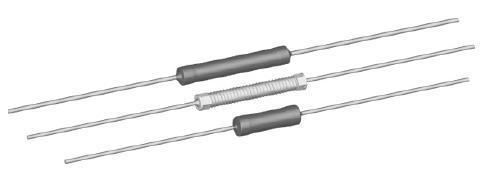
Wirewound Resistors - Through Hole 5watts 10ohms 10%
The input terminals shown in the block diagram of the CA5130 Series CMOS Operational Amplifiers may be operated down to 0.5V below the negative supply rail, and the output can be swung very close to either supply rail in many applications. Consequently, the CA5130 Series circuits are ideal for single supply operation. Three Class A amplifier stages, having the individual gain capability and current consumption shown in the Block Diagram, provide the total gain of the CA5130. A biasing circuit provides two potentials for common use in the first and second stages. Terminal 8 can be used both for phase compensation and to strobe the output stage into quiescence.
When Terminal 8 is tied to the negative supply rail (Terminal 4) by mechanical or electrical means, the output potential at Terminal 6 essentially rises to the positive supply rail potential at Terminal 7. This condition of essentially zero current drain in the output stage under the strobed "OFF" condition can only be achieved when the ohmic load resistance presented to the amplifier is very high (e.g., when CA5130 amplifier output is used to drive CMOS digital circuits in comparator applications).