Features: • High Input Resistance . . . . . . . . . . . . . . . . . . .2TW (Typ)• Standby Power at V+ = 5V . . . . . . . . . . . . . 300nW (Typ)• Supply Current, BW, Slew Rate Programmable Using External Resistor• Input Current . . . . . . . . . . . . . . . . . . . . . . . ...
CA3440: Features: • High Input Resistance . . . . . . . . . . . . . . . . . . .2TW (Typ)• Standby Power at V+ = 5V . . . . . . . . . . . . . 300nW (Typ)• Supply Current, BW, Slew Rate Prog...
SeekIC Buyer Protection PLUS - newly updated for 2013!
268 Transactions
All payment methods are secure and covered by SeekIC Buyer Protection PLUS.
The CA3440 is an integrated circuit operational amplifier that combines the advantages of MOS and bipolar transistors on a single monolithic chip.
The CA3440 BiMOS op amp features gate protected PMOS transistors in the input circuit to provide very high input impedance, very low input currents (less than 10pA). CA3440 operates at total supply voltages from 5V to 15V and can be operated over the temperature range from -55 to 125. The virtues are programmability and very low standby power consumption (300nW). This operational amplifier is internally phase compensated to achieve stable operation in the unity gain follower configuration. Terminals are also provided for use in applications requiring input offset voltage nulling. The use of PMOS in the input stage results in common mode input voltage capability down to 0.5V below the negative supply terminals, an important attribute for single supply applications. CA3440 output stage uses MOS complementary source follower form which permits moderate load driving capability (10kW) at very low standby currents (50nA).
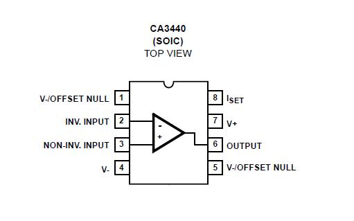
The CA3440 has the same 8 lead pinout as the "741" and other industry standard op amps with two exceptions: terminals one and five must be connected to the negative supply or to a potentiometer if nulling is required. Terminal 8 must be programmed through an external resistor returned to the negative supply.