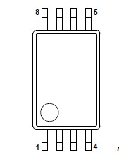
Features: · 40 mW on-state resistance at 2.5 V gate drive· RDSon rating down to 1.8 V· ESD gate protectionApplication· Li-Ion safety switch· Power managePinoutSpecifications SYMBOL PARAMETER CONDITIONS MIN. MAX. UNIT Per FET VDS drain-source voltage (DC) ...
BSH301: Features: · 40 mW on-state resistance at 2.5 V gate drive· RDSon rating down to 1.8 V· ESD gate protectionApplication· Li-Ion safety switch· Power managePinoutSpecifications SYMBOL PARAMET...
SeekIC Buyer Protection PLUS - newly updated for 2013!
268 Transactions
All payment methods are secure and covered by SeekIC Buyer Protection PLUS.
SYMBOL |
PARAMETER |
CONDITIONS |
MIN. |
MAX. |
UNIT |
Per FET | |||||
VDS |
drain-source voltage (DC) |
20 |
V | ||
VGSO |
gate-source voltage (DC) |
|
±8 |
V | |
ID |
drain current (DC) |
Ts = 80 °C; note 1 |
5 |
A | |
IDM |
peak drain current |
note 2 |
20 |
A | |
Ptot |
total power dissipation |
TS = 80 °C; note 3 |
1.75 |
W | |
Tamb = 25 °C; note 4 |
1.85 |
W | |||
Tamb = 25 °C; note 5 |
0.95 |
W | |||
Tstg |
storage temperature |
-55 |
+150 |
°C | |
Tj |
operating junction temperature |
-55 |
+150 |
°C |
1. TS is the temperature at the soldering point of the drain lead.
2. Pulse width and duty cycle limited by maximum junction temperature.
3. Maximum permissible dissipation per transistor. Both devices may be loaded up to 3.5 W at the same time.
4. Maximum permissible dissipation per transistor. Device mounted on a printed-circuit board with R th a-tp (ambient to tie-point) of 27.5 °C/W.
5. Maximum permissible dissipation per transistor. Device mounted on a printed-circuit board with R th a-tp (ambient to tie-point) of 90 °C/W.