Transistor Polarity
: N-Channel
Maximum Operating Temperature
: + 150 C
Configuration
: Dual
Drain-Source Breakdown Voltage
: 65 V
Gate-Source Breakdown Voltage
: +/- 20 V
Continuous Drain Current
: 9 A
Packaging
: Bulk
Frequency
: 500 MHz
Gain
: 13 dB
Output Power
: 80 W
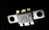
Package / Case
: SOT-268A
Features: * High power gain
* Easy power control
* Good thermal stability
* Gold metallization ensures excellent reliability
* Designed for broadband operation.Pinout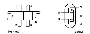 Specifications
| SYMBOL |
PARAMETER |
CONDITIONS |
MIN. |
MAX. |
UNIT |
| VDS |
drain-source voltage |
|
|
65 |
V |
| VGS |
gate-source voltage |
|
|
20 |
V |
| ID |
DC drain current |
|
|
9 |
A |
| Ptot |
total power dissipation |
up to Tmb =25 °C; total device;
both sections equally loaded |
|
125 |
W |
| Tstg |
storage temperature |
|
-65 |
150 |
C |
| Tj |
junction temperature |
|
|
200 |
C |
|
|
|
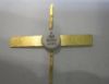
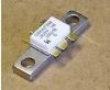
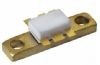
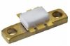
DescriptionThe BLF546 is a type of UHF push-pull powewr mos transistor.Silicon N-channel enhancement mode vertical D-MOS push-pull transistor applied for communications transmitter applications in the UHF frequency range. The transistor BLF546 is encapsulated in a 4-lead, SOT268 balanced flange envelope, with two ceramic caps. The mounting flange offers the common source connection for the transistors.
The BLF546 has the following features:(1)High power gain;(2)Easy power control;(3)Good thermal stability;(4)Gold metallization ensures,excellent reliability;(5)Designed for broadband operation.
BLF546 also has some outstanding limiting values(In accordance with the absolute maximum System ,Per transistor of BLF546 secti on unless otherwise specified.) and electrical characteristics(Tj=25°C).Absolute maximum ratings:(1):drain-source voltage is 65 V max;(2):gate-source voltage is 20 V max;(3):drain current is 9 A max;(4): total power dissipation is 145 W max(up to Tmb = 25 °C; total device;both sections equally loaded);(5): storage temperature is 65 to 150 °C;(6): junction temperature is 200 °C max.characteristics:(1):drain-source breakdown voltage is 65 V min when VGS is 0 and ID is 20 mA;(2):drain-source leakage current is 2 mA max when VGS is 0 and VDS is 28 V;(3): gate-sour ce leakage current is 1 mA max when ±VGS is 20 V and VDS is 0 ;(4): gate-source threshold voltage is 1 V min and 4 V max when ID is 80 mA and VDS is 10 V;(5):forward transconductance is 1.2 s min and 1.7 s typ when ID is 2.4 A and VDS is 10 V;(6):drain-source on-state resistance is 0.4 typ and 0.6 max when ID is 2.4 An and VGS is 10 V;(7):on-state drain current is 10 A typ when VGS is 15 V and VDS is 10 V;(8): input capacitance is 60 pF when VGS is 0 , VDS is 28 V and f is 1 MHz;(9): output capacitance is 46 pF when VGS is 0, VDS is 28 V and f is 1 MHz.etc.

 BLF546 Data Sheet