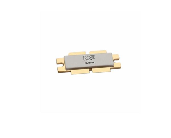
Features: · High power gain· Low intermodulation distortion· Easy power control· Good thermal stability· Withstands full load mismatch.Specifications SYMBOL PARAMETER CONDITIONS MIN. MAX. UNIT VDS drain-source voltage 65 V VGS gate-source voltage 20 ...
BLF147: Features: · High power gain· Low intermodulation distortion· Easy power control· Good thermal stability· Withstands full load mismatch.Specifications SYMBOL PARAMETER CONDITIONS...
SeekIC Buyer Protection PLUS - newly updated for 2013!
268 Transactions
All payment methods are secure and covered by SeekIC Buyer Protection PLUS.
SYMBOL | PARAMETER | CONDITIONS | MIN. | MAX. | UNIT |
VDS | drain-source voltage | 65 | V | ||
VGS | gate-source voltage | 20 | V | ||
ID | DC drain current | 25 | A | ||
Ptot | total power dissipation | up to Tmb = 25 C; total device;both sections equally loaded | 220 | W | |
Tstg | storage temperature | -65 | 150 | C | |
Tj | junction temperature | 200 | C | ||
Silicon N-channel enhancement mode vertical D-MOS transistor BLF147 designed for industrial and military applications in the HF/VHF frequency range.
The transistor BLF147 is encapsulated in a 4-lead, SOT121 flange envelope, with a ceramic cap. All leads are isolated
from the flange.
The BLF147 is a marking code, showing gate-source voltage (VGS) information is provided for matched pair applications. Refer to 'General' section for further information.