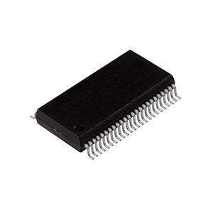
B5S16862

Features: ` HIGH SPEED: tPD = 0.25ns (MAX.) at VCC = 4.5V TA=85` ON RESISTANCE BETWEEN TWO PORT: 5 (TYP) at VCC = 5.0V TA=25` LOW POWER DISSIPATION: ICC = 1uA(MAX.) at TA=25` COMPATIBLE WITH TTL OUTPUTS: VIH=2V(MIN), VIL=0.8V(MAX)` POWER DOWN PROTECTION ON INPUTS AND OUTPUTS` OPERATING VOLTAGE RAN...

product image

B5S16862 Picture
SeekIC No. : 004294915 Detail

B5S16862: Features: ` HIGH SPEED: tPD = 0.25ns (MAX.) at VCC = 4.5V TA=85` ON RESISTANCE BETWEEN TWO PORT: 5 (TYP) at VCC = 5.0V TA=25` LOW POWER DISSIPATION: ICC = 1uA(MAX.) at TA=25` COMPATIBLE WITH TTL OUT...

floor Price/Ceiling Price

Part Number:
B5S16862
Supply Ability:
5000

Price Break

  • Qty
  • 1~5000
  • Unit Price
  • Negotiable
  • Processing time
  • 15 Days
Total Cost: $ 0.00

SeekIC Buyer Protection PLUS - newly updated for 2013!

  • Escrow Protection.
  • Guaranteed refunds.
  • Secure payments.
  • Learn more >>

Month Sales

268 Transactions

Rating

evaluate  (4.8 stars)

Upload time: 2024/11/21

Payment Methods

All payment methods are secure and covered by SeekIC Buyer Protection PLUS.

Notice: When you place an order, your payment is made to SeekIC and not to your seller. SeekIC only pays the seller after confirming you have received your order. We will also never share your payment details with your seller.
Product Details

Description


Features:

` HIGH SPEED: tPD = 0.25ns (MAX.) at VCC = 4.5V TA=85
` ON RESISTANCE BETWEEN TWO PORT: 5 (TYP) at VCC = 5.0V TA=25
` LOW POWER DISSIPATION: ICC = 1uA(MAX.) at TA=25
` COMPATIBLE WITH TTL OUTPUTS: VIH=2V(MIN), VIL=0.8V(MAX)
` POWER DOWN PROTECTION ON INPUTS AND OUTPUTS
` OPERATING VOLTAGE RANGE: VCC(OPR) = 4V to 5.5V
` PIN AND FUNCTION COMPATIBLE WITH 74 SERIES 16862
` IMPROVED LATCH-UP IMMUNITY
` ESD PERFORMANCE:
    HBM > 2000V (MIL STD 883 method 3015);
    MM > 200V


Pinout

  Connection Diagram


Specifications

Symbol
Parameter2
Value
Unit
VCC
Supply Voltage
-0.5 to +7.0
V
VI
DC Switch and Control Pin Voltage
-0.5 to +7.0
V
VO
DC Output Voltage (VCC = 0V) (note 1)
-0.5 to +7.0
V
VO
DC Output Voltage (VI/O=Gnd)
-0.5 to +7.0
V
IIK
DC Input Diode Current (VI/O < 0V)
-50
mA
IOK
DC Output Diode Current (note 2)
-50
mA
IO
DC Output Current (note 3)
128
mA
ICC or IGND
DC VCC or Ground Current per Supply Pin
±100
mA
Tstg
Storage Temperature
-65 to +150
TL
Lead Temperature (10 sec)
300
Absolute Maximum Ratings are those values beyond which damage to the device may occur. Functional
operation under these conditions is not implied

1) IO absolute maximum rating must be observed
2) VO < GND,VO > VCC
3) Not more than one output should be tested at one time. Duration of the test should not exceed one second.


Description

The B5S16862 is an advanced high-speed CMOS 20-BIT TWO PORT BUS SWITCH fabricated with sub-micron silicon gate and double-layer metal wiring C2MOS tecnology.

It is ideal for 4V to 5.5V VCC operations and ultra-low power and low noise applications, typically notebook and docking station.

Any nG output control governs four 5-bit BUS SWITCHES. Output Enable inputs (nG) tied together gives full 20-bit operations. When nG is LOW, the switches are on. When nG is HIGH, the switches are in high impedance state.

It has ultra high-speed performance at 5V near zero delay with low ON resistance.

All inputs and outputs are equipped with protection circuits against static discharge, giving them 2KV ESD immunity and transient excess voltage.


Customers Who Bought This Item Also Bought

Margin,quality,low-cost products with low minimum orders. Secure your online payments with SeekIC Buyer Protection.
Integrated Circuits (ICs)
Soldering, Desoldering, Rework Products
Resistors
RF and RFID
Hardware, Fasteners, Accessories
Inductors, Coils, Chokes
View more