Features: The Am29SL400C is an 4Mbit, 1.8 V volt-only Flash memory organized as 524,288 bytes or 262,144 words. The device is offered in 48-pin TSOP and 48-ball FBGA packages. The word-wide data (x16) appears on DQ15DQ0; the byte-wide (x8) data appearson DQ7DQ0. This device is designed to be progr...
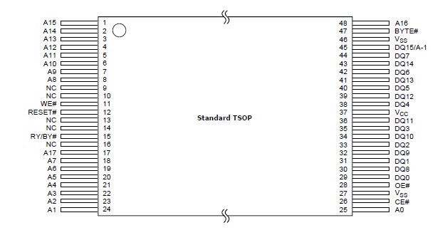
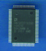
Am29SL400C: Features: The Am29SL400C is an 4Mbit, 1.8 V volt-only Flash memory organized as 524,288 bytes or 262,144 words. The device is offered in 48-pin TSOP and 48-ball FBGA packages. The word-wide data (x1...
SeekIC Buyer Protection PLUS - newly updated for 2013!
268 Transactions
All payment methods are secure and covered by SeekIC Buyer Protection PLUS.
The Am29SL400C is an 4Mbit, 1.8 V volt-only Flash memory organized as 524,288 bytes or 262,144 words. The device is offered in 48-pin TSOP and 48-ball FBGA packages. The word-wide data (x16) appears on DQ15DQ0; the byte-wide (x8) data appearson DQ7DQ0. This device is designed to be programmed and erased in-system with a single 1.8 volt VCC supply. No VPP is required for write or erase operations. The device can also be programmed in standard EPROM programmers.
The standard device offers access times of 100, 110, 120, and 150 ns, allowing high speed microprocessors to operate without wait states. To eliminate bus contention the device has separate chip enable (CE#), write enable (WE#) and output enable (OE#) controls.
The device requires only a single 1.8 volt power supply for both read and write functions. Internally generated and regulated voltages are provided for the program and erase operations.
The device is entirely command set compatible with the JEDEC single-power supply Flash standard. Commands are written to the command register using standard microprocessor write timings. Register contents serve as input to an internal state-machine that controls the erase and programming circuitry. Write cycles also internally latch addresses and data needed for the programming and erase operations. Reading data out of the device is similar to reading from other Flash or EPROM devices.
Device programming occurs by executing the program command sequence. This initiates the Embedded Program algorithm-an internal algorithm that automatically times the program pulse widths and verifies proper cell margin. The Unlock Bypass mode facilitates faster programming times by requiring only two write cycles to program data instead of four.