Pinout Specifications
Storage Temperature
Plastic Packages . . . . . . . . . . . . . . .65°C to +150°C
Ambient Temperature
with Power Applied. . . . . . . . . . . . . 55°C to +125°C
Voltage with Respect to Ground
VCC (Note 1). . . . . . . . . . . . . . . . . ......2.0 V to 7.0 V
A9, OE#, RESET# (Note 2) . . . . ........2.0 V to 13.0 V
All other pins (Note 1) . . . . . . . . . . .....2.0 V to 7.0 V
Output Short Circuit Current (Note 3) . . . . .. . 200 mA
Notes:
1. Minimum DC voltage on input or I/O pins is 0.5 V. During voltage transitions, inputs may overshoot VSS to 2.0 V for periods of up to 20 ns. See Figure 6. Maximum DC voltage on output and I/O pins is VCC + 0.5 V. During voltage transitions, outputs may overshoot to VCC + 2.0 V for periods up to 20 ns. See Figure 7.
2. Minimum DC input voltage on A9, OE#, RESET# pins is 0.5V. During voltage transitions, A9, OE#, RESET# pins may overshoot VSS to 2.0 V for periods of up to 20 ns. See Figure 6. Maximum DC input voltage on A9, OE#, and RESET# is 13.0 V which may overshoot to 13.5 V for periods up to 20 ns.
3. No more than one output shorted at a time. Duration of the short circuit should not be greater than one second.
Stresses greater than those listed in this section may cause permanent damage to the device. This is a stress rating only; functional operation of the device at these or any other conditions above those indicated in the operational sections of this specification is not implied. Exposure of the device to absolute maximum rating conditions for extended periods may affect device reliability.
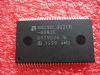
DescriptionThe Am29F032B is a 32 Mbit, 5.0 volt-only Flash memory organized as 4,194,304 bytes of 8 bits each. The 4 Mbytes of data are divided into 64 sectors of 64 Kbytes each for flexible erase capability. The 8 bits of data appear on DQ0DQ7. The Am29F032B is offered in 40-pin TSOP and 44-pin SO packages. The Am29F032B is manufactured using AMD's 0.32 m process technology. This device is designed to be programmed in-system with the standard system 5.0 volt VCC supply. A 12.0 volt VPP is not required for program or erase operations. The device can also be programmed in standard EPROM programmers.
The standard device offers access times of 70, 90, 120, and 150 ns, allowing high-speed microprocessors to operate without wait states. To eliminate bus contention, the device has separate chip enable (CE#), write enable (WE#), and output enable (OE#) controls.
Am29F032B is entirely command set compatible with the JEDEC single-power-supply Flash standard. Commands are written to the command register using standard microprocessor write timings. Register contents serve as input to an internal state machine that controls the erase and programming circuitry. Write cycles also internally latch addresses and data needed for the programming and erase operations. Reading data out of the device is similar to reading from 12.0 volt Flash or EPROM devices.
Am29F032B is programmed by executing the program command sequence. This invokes the Embedded Program algorithm-an internal algorithm that automatically times the program pulse widths and verifies proper cell margin. The device is erased by executing the erase command sequence. This invokes the Embedded Erase algorithm-an internal algorithm that automatically preprograms the array (if it is not already programmed) before executing the erase operation. During erase, the device automatically times the erase pulse widths and verifies proper cell margin.
The sector erase architecture allows memory sectors to be erased and reprogrammed without affecting the data contents of other sectors. A sector is typically erased and verified within one second. The device is erased when shipped from the factory.
The hardware sector group protection feature disables both program and erase operations in any combination of the eight sector groups of memory. A sector group consists of four adjacent sectors.
The Erase Suspend feature enables the system to put erase on hold for any period of time to read data from, or program data to, a sector that is not being erased. True background erase can thus be achieved.
Am29F032B requires only a single 5.0 volt power supply for both read and write functions. Internally generated and regulated voltages are provided for the program and erase operations. A low VCC detector automatically inhibits write operations during power transitions. The host system can detect whether a program or erase cycle is complete by using the RY/BY# pin, the DQ7 (Data# Polling) or DQ6 (toggle) status bits. After a program or erase cycle has been completed, the device automatically returns to the read mode.
A hardware RESET# pin terminates any operation in progress. The internal state machine is reset to the read mode. The RESET# pin may be tied to the system reset circuitry. Therefore, if a system reset occurs during either an Embedded Program or Embedded Erase algorithm, the device is automatically reset to the read mode. This enables the system's microprocessor to read the boot-up firmware from the Flash memory.
AMD's Flash technology combines years of Flash memory manufacturing experience to produce the highest levels of quali ty, rel iabi l i ty, and cost effectiveness. The device electrically erases all bits within a sector simultaneously via Fowler-Nordheim tunneling. The bytes are programmed one byte at a time using the programming mechanism of hot electron injection.

 Am29F032B Data Sheet